CY28442ZXC Cypress Semiconductor Corp, CY28442ZXC Datasheet - Page 9
CY28442ZXC
Manufacturer Part Number
CY28442ZXC
Description
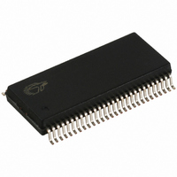
IC CLOCK GEN ALVISO 56-TSSOP
Manufacturer
Cypress Semiconductor Corp
Type
Fanout Distribution, Spread Spectrum Clock Generatorr
Datasheet
1.CY28442ZXC.pdf
(22 pages)
Specifications of CY28442ZXC
Pll
Yes with Bypass
Input
LVTTL, Crystal
Output
Clock
Number Of Circuits
1
Ratio - Input:output
11:15
Differential - Input:output
No/Yes
Frequency - Max
200MHz
Divider/multiplier
Yes/No
Voltage - Supply
3.135 V ~ 3.465 V
Operating Temperature
0°C ~ 85°C
Mounting Type
Surface Mount
Package / Case
56-TSSOP II
Frequency-max
100MHz
Lead Free Status / RoHS Status
Lead free / RoHS Compliant
Available stocks
Company
Part Number
Manufacturer
Quantity
Price

Part Number:
CY28442ZXC-2
Manufacturer:
CYP
Quantity:
20 000
Company:
Part Number:
CY28442ZXC-2T
Manufacturer:
TI
Quantity:
11
Company:
Part Number:
CY28442ZXC-4
Manufacturer:
SEMTEC
Quantity:
946


Document #: 38-07680 Rev. **
Byte 10: Control Register 10 (continued)
The CY28442 requires a Parallel Resonance Crystal. Substi-
tuting a series resonance crystal will cause the CY28442 to
operate at the wrong frequency and violate the ppm specifi-
cation. For most applications there is a 300-ppm frequency
shift between series and parallel crystals due to incorrect
loading.
Table 5. Crystal Recommendations
Crystal Loading
Crystal loading plays a critical role in achieving low ppm perfor-
mance. To realize low ppm performance, the total capacitance
the crystal will see must be considered to calculate the appro-
priate capacitive loading (CL).
Calculating Load Capacitors
In addition to the standard external trim capacitors, trace
capacitance and pin capacitance must also be considered to
correctly calculate crystal loading. As mentioned previously,
the capacitance on each side of the crystal is in series with the
2
1
0
14.31818 MHz
Frequency
Bit
(Fund)
@Pup
0
0
0
Cut
AT
CLKREQ#A
CLKREQ#A
CLKREQ#A
Loading Load Cap
Parallel
Name
ADVANCE INFORMATION
Figure 1. Crystal Capacitive Clarification
20 pF
0.1 mW
SRC[T/C]5 CLKREQ#A control
1 = SRC[T/C]5 stoppable by CLKREQ#A pin
0 = SRC[T/C]5 not controlled by CLKREQ#A pin
SRC[T/C]3 CLKREQ#A control
1 = SRC[T/C]3 stoppable by CLKREQ#A pin
0 = SRC[T/C]3 not controlled by CLKREQ#A pin
SRC[T/C]1 CLKREQ#A control
1 = SRC[T/C]1 stoppable by CLKREQ#A pin
0 = SRC[T/C]1 not controlled by CLKREQ#A pin
(max.)
Drive
Shunt Cap
The following diagram shows a typical crystal configuration
using the two trim capacitors. An important clarification for the
following discussion is that the trim capacitors are in series
with the crystal not parallel. It’s a common misconception that
load capacitors are in parallel with the crystal and should be
approximately equal to the load capacitance of the crystal.
This is not true.
crystal. This means the total capacitance on each side of the
crystal must be twice the specified crystal load capacitance
(CL). While the capacitance on each side of the crystal is in
series with the crystal, trim capacitors (Ce1,Ce2) should be
calculated to provide equal capacitive loading on both sides.
(max.)
5 pF
Motional
0.016 pF
(max.)
Description
Tolerance
35 ppm
(max.)
Stability
30 ppm
(max.)
CY28442
Page 9 of 22
Aging
(max.)
5 ppm
[+] Feedback
Related parts for CY28442ZXC
Image
Part Number
Description
Manufacturer
Datasheet
Request
R

Part Number:
Description:
Manufacturer:
Cypress Semiconductor Corp
Datasheet:
Part Number:
Description:
Manufacturer:
Cypress Semiconductor Corp
Datasheet:
Part Number:
Description:
Manufacturer:
Cypress Semiconductor Corp
Datasheet:
Part Number:
Description:
Manufacturer:
Cypress Semiconductor Corp
Datasheet:
Part Number:
Description:
Manufacturer:
Cypress Semiconductor Corp
Datasheet: