MC88915TFN70 Freescale Semiconductor, MC88915TFN70 Datasheet - Page 11
MC88915TFN70
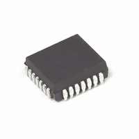
Manufacturer Part Number
MC88915TFN70
Description
IC DRIVER CLK PLL 70MHZ 28-PLCC
Manufacturer
Freescale Semiconductor
Type
Clock Driver, Fanout Distribution, Multiplexerr
Datasheet
1.MC88915TFN70R2.pdf
(21 pages)
Specifications of MC88915TFN70
Pll
Yes
Input
TTL
Output
CMOS, TTL
Number Of Circuits
1
Ratio - Input:output
3:8
Differential - Input:output
No/No
Frequency - Max
70MHz
Divider/multiplier
Yes/Yes
Voltage - Supply
4.75 V ~ 5.25 V
Operating Temperature
0°C ~ 70°C
Mounting Type
Surface Mount
Package / Case
28-PLCC
Frequency-max
70MHz
Lead Free Status / RoHS Status
Contains lead / RoHS non-compliant
Available stocks
Company
Part Number
Manufacturer
Quantity
Price
Company:

Part Number:
MC88915TFN70
Manufacturer:
ON
Quantity:
11
Company:
Part Number:
MC88915TFN70
Manufacturer:
MOT
Quantity:
5 510
Company:
Part Number:
MC88915TFN70
Manufacturer:
Freescale Semiconductor
Quantity:
10 000
Part Number:
MC88915TFN70
Manufacturer:
N/A
Quantity:
20 000
Company:
Part Number:
MC88915TFN70R2
Manufacturer:
Freescale Semiconductor
Quantity:
10 000


AC CHARACTERISTICS
1. T
2. The T
3. Under equally loaded conditions and at a fixed temperature and voltage.
4. With V
5. The t
t
Outputs
t
2X_Q Output
t
(Q0–Q4, Q5, Q/2)
t
(2X_Q Output)
t
SYNC Feedback
SYNC Feedback
t
(2x_Q Output)
t
(Rising) See Note 4
t
(Falling)
t
t
t
t
RISE/FALL
RISE/FALL
PULSE WIDTH
PULSE WIDTH
PD
CYCLE
SKEWr
SKEWf
SKEWall
LOCK
PZL
PHZ
MOTOROLA
C1 = 0.01 F.
1
CYCLE
5
,t
4
PLZ
Symbol
3
3
PZL
3
PD
CC
5
in this spec is 1/Frequency at which the particular output is running.
, t
specification’s min/max values may shift closer to zero if a larger pullup resistor is used.
fully powered–on, and an output properly connected to the FEEDBACK pin. t
PHZ
, t
PLZ
minimum and maximum specifications are estimates, the final guaranteed values will be available when ‘MC’ status is reached.
Rise/Fall Time, All Outputs
(Between 0.2V
Rise/Fall Time
Output Pulse Width: Q0, Q1, Q2, Q3, Q4,
Q5, Q/2 @ V
Output Pulse Width:
2X_Q @ V
SYNC Input to Feedback Delay
(Measured at SYNC0 or 1 and
(Measured at SYNC0 or 1 and
FEEDBACK Input Pins)
Cycle–to–Cycle Variation
Output–to–Output Skew Between Outputs
Q0–Q4, Q/2 (Rising Edges Only)
Output–to–Output Skew Between Outputs
Q0–Q4 (Falling Edges Only)
Output–to–Output Skew 2X_Q, Q/2,
Q0–Q4 Rising, Q5 Falling
Time Required to Acquire Phase–Lock
From Time SYNC Input Signal is
Received
Output Enable Time OE/RST to 2X_Q,
Q0–Q4, Q5, and Q/2
Output Disable Time OE/RST to 2X_Q,
Q0–Q4, Q5, and Q/2
(T
A
=0 C to +70 C, V
CC
CC
CC
Parameter
/2
and 0.8V
MC88915TFN160
CC
CC
)
= 5.0V 5%, Load = 50 Terminated to V
100MHz
133MHz
160MHz
133MHz
160MHz
133MHz
160MHz
80MHz
0.5t
0.5t
0.5t
0.5t
t
t
CYCLE
CYCLE
(With 1M from RC1 to An V
CYCLE
CYCLE
CYCLE
CYCLE
–1.05
TBD
–0.9
Min
1.0
0.5
1.0
3.0
3.0
—
—
—
– 300ps
– 300ps
(continued)
– 0.5
– 0.7
– 0.5
– 0.5
2
LOCK
0.5t
0.5t
0.5t
0.5t
t
t
CYCLE
CYCLE
maximum is with C1 = 0.1 F, t
CYCLE
CC
CYCLE
CYCLE
CYCLE
–0.25
–0.10
TBD
Max
500
500
750
/2)
2.5
1.6
10
14
14
+ 300ps
+ 300ps
+ 0.5
CC
+ 0.7
+ 0.5
+ 0.5
)
2
Unit
ms
ns
ns
ns
ns
ns
ps
ps
ps
ns
ns
Into a 50 Load
Terminated to V
t
t
Into a 50 Load
Terminated to V
See Note 2 and
Figure 2 for Detailed
Figure 2 for Detailed
Explanation
All Outputs Into a
Matched 50 Load
Terminated to V
All Outputs Into a
Matched 50 Load
Terminated to V
All Outputs Into a
Matched 50 Load
Terminated to V
Also Time to LOCK
Indicator High
Measured With the
PLL_EN Pin Low
Measured With the
PLL_EN Pin Low
RISE
FALL
LOCK
: 0.8V – 2.0V
: 2.0V – 0.8V
Condition
minimum is with
CC
CC
CC
CC
CC
11
/2
/2
/2
/2
/2
Related parts for MC88915TFN70
Image
Part Number
Description
Manufacturer
Datasheet
Request
R

Part Number:
Description:
Manufacturer:
Freescale Semiconductor, Inc
Datasheet:
Part Number:
Description:
Manufacturer:
Freescale Semiconductor, Inc
Datasheet:
Part Number:
Description:
Manufacturer:
Freescale Semiconductor, Inc
Datasheet:
Part Number:
Description:
Manufacturer:
Freescale Semiconductor, Inc
Datasheet:
Part Number:
Description:
Manufacturer:
Freescale Semiconductor, Inc
Datasheet:
Part Number:
Description:
Manufacturer:
Freescale Semiconductor, Inc
Datasheet:
Part Number:
Description:
Manufacturer:
Freescale Semiconductor, Inc
Datasheet:
Part Number:
Description:
Manufacturer:
Freescale Semiconductor, Inc
Datasheet:
Part Number:
Description:
Manufacturer:
Freescale Semiconductor, Inc
Datasheet:
Part Number:
Description:
Manufacturer:
Freescale Semiconductor, Inc
Datasheet:
Part Number:
Description:
Manufacturer:
Freescale Semiconductor, Inc
Datasheet:
Part Number:
Description:
Manufacturer:
Freescale Semiconductor, Inc
Datasheet:
Part Number:
Description:
Manufacturer:
Freescale Semiconductor, Inc
Datasheet:
Part Number:
Description:
Manufacturer:
Freescale Semiconductor, Inc
Datasheet:
Part Number:
Description:
Manufacturer:
Freescale Semiconductor, Inc
Datasheet: