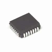
MC88915TFN70 Freescale Semiconductor, MC88915TFN70 Datasheet - Page 8

MC88915TFN70
Manufacturer Part Number
MC88915TFN70
Description
IC DRIVER CLK PLL 70MHZ 28-PLCC
Manufacturer
Freescale Semiconductor
Type
Clock Driver, Fanout Distribution, Multiplexerr
Datasheet
1.MC88915TFN70R2.pdf
(21 pages)
Specifications of MC88915TFN70
Pll
Yes
Input
TTL
Output
CMOS, TTL
Number Of Circuits
1
Ratio - Input:output
3:8
Differential - Input:output
No/No
Frequency - Max
70MHz
Divider/multiplier
Yes/Yes
Voltage - Supply
4.75 V ~ 5.25 V
Operating Temperature
0°C ~ 70°C
Mounting Type
Surface Mount
Package / Case
28-PLCC
Frequency-max
70MHz
Lead Free Status / RoHS Status
Contains lead / RoHS non-compliant
Available stocks
Company
Part Number
Manufacturer
Quantity
Price
Company:
Part Number:
MC88915TFN70
Manufacturer:
ON
Quantity:
11
Company:
Part Number:
MC88915TFN70
Manufacturer:
MOT
Quantity:
5 510
Company:
Part Number:
MC88915TFN70
Manufacturer:
Freescale Semiconductor
Quantity:
10 000
Part Number:
MC88915TFN70
Manufacturer:
N/A
Quantity:
20 000
Company:
Part Number:
MC88915TFN70R2
Manufacturer:
Freescale Semiconductor
Quantity:
10 000
SYNC INPUT TIMING REQUIREMENTS
1. These t
2. Information in Table 1 and in Note 3 of the AC specification notes describe this specification and its limits depending on what output is fed back,
DC ELECTRICAL CHARACTERISTICS
1. I
2. The PLL_EN input pin is not guaranteed to meet this specification.
3. Maximum test duration is 2.0ms, one output loaded at a time.
4. Specification value for I
CAPACITANCE AND POWER SPECIFICATIONS
NOTE: PD
FREQUENCY SPECIFICATIONS
1. Maximum Operating Frequency is guaranteed with the part in a phase–locked condition, and all outputs loaded with 50 terminated to V
t
t
Duty Cycle SYNC Inputs
Symbol
RISE/FALL
CYCLE
Symbol
8
I
Figure 5b.
and if FREQ_SEL
I
I
V
V
V
OHD
I
f
V
CCT
OLD
I
OL
max
I
CC
OZ
OH
OL
in
IH
IL
Symbol
and I
, SYNC Inputs
C
PD
PD
1
C
PD
Symbol
IN
1
CYCLE
,SYNC Inputs
1
2
OH
and PD
Minimum High–Level Input
Voltage
Maximum Low–Level Input
Voltage
Minimum High–Level Output
Voltage
Maximum Low–Level Output
Voltage
Maximum Input Leakage Current
Maximum I
Minimum Dynamic Output Current
Maximum Quiescent Supply
Current (per Package)
Maximum 3–State Leakage Current
Maximum Operating Frequency (2X_Q Output)
Maximum Operating Frequency (Q0–Q4,Q5 Output)
are 12mA and –12mA respectively for the LOCK output.
minimum values are valid when ‘Q’ output is fed back and connected to the FEEDBACK pin. This is the configuration shown in
2
mW/Output numbers are for a ‘Q’ output.
Input Capacitance
Power Dissipation Capacitance
Power Dissipation @ 50MHz with 50
Power Dissipation @ 50MHz with 50
is high or low.
CC
OZ
/Input
is preliminary, will be finalized upon ‘MC’ status.
Rise/Fall Time, SYNC Inputs From 0.8 to 2.0V
Input Clock Period SYNC Inputs
Input Duty Cycle SYNC Inputs
Parameter
(T
A
=–40 C to +85 C, V
(Voltages Referenced to GND) T
3
Parameter
Parameter
MC88915TFN133
Parameter
Thevenin Termination
Parallel Termination to GND
V
V
V
V
V
V
V
V
V
V
I
I
CC
out
out
OH
OL
in
in
I
I
OLD
OHD
I
I
= V
= V
= V
= V
= V
= V
= 5.0 V 5%)
= 36 mA
= 0.1 V or V
= 0.1 V or V
= –36 mA
= 1.0V Max
CC
CC
CC
IH
= 3.85V Min
IH
IH
or V
Test Conditions
or GND
– 2.1 V
or GND
or V
or V
IL
1
IL
IL
;V
1
A
O
CC
CC
=–40 C to +85 C, V
= V
– 0.1 V
– 0.1 V
CC
or GND
Typical Values
184mW/Device
456mW/Device
23mW/Output
57mW/Output
CC
4.75
5.25
4.75
5.25
4.75
5.25
4.75
5.25
5.25
5.25
5.25
5.25
5.25
5.25
4.5
V
40
Guaranteed Minimum
V
CC
= 5.0 V
Minimum
15.0
—
TFN133
133
1
66
50% 25%
5%
Target Limit
Unit
mW
mW
pF
pF
4.01
4.51
0.44
0.44
2.0
–88
2.0
2.0
0.8
0.8
1.0
50
88
1.0
Maximum
2
4
100
3.0
MOTOROLA
V
V
V
V
Conditions
2
T = 25 C
CC
CC
CC
T = 25 C
CC
= 5.0 V
= 5.0 V
= 5.0 V
= 5.0 V
MHz
MHz
Unit
Unit
Unit
mA
mA
mA
mA
CC
ns
ns
V
V
V
V
A
A
/2.


