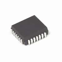
MC88915TFN70 Freescale Semiconductor, MC88915TFN70 Datasheet - Page 14

MC88915TFN70
Manufacturer Part Number
MC88915TFN70
Description
IC DRIVER CLK PLL 70MHZ 28-PLCC
Manufacturer
Freescale Semiconductor
Type
Clock Driver, Fanout Distribution, Multiplexerr
Datasheet
1.MC88915TFN70R2.pdf
(21 pages)
Specifications of MC88915TFN70
Pll
Yes
Input
TTL
Output
CMOS, TTL
Number Of Circuits
1
Ratio - Input:output
3:8
Differential - Input:output
No/No
Frequency - Max
70MHz
Divider/multiplier
Yes/Yes
Voltage - Supply
4.75 V ~ 5.25 V
Operating Temperature
0°C ~ 70°C
Mounting Type
Surface Mount
Package / Case
28-PLCC
Frequency-max
70MHz
Lead Free Status / RoHS Status
Contains lead / RoHS non-compliant
Available stocks
Company
Part Number
Manufacturer
Quantity
Price
Company:
Part Number:
MC88915TFN70
Manufacturer:
ON
Quantity:
11
Company:
Part Number:
MC88915TFN70
Manufacturer:
MOT
Quantity:
5 510
Company:
Part Number:
MC88915TFN70
Manufacturer:
Freescale Semiconductor
Quantity:
10 000
Part Number:
MC88915TFN70
Manufacturer:
N/A
Quantity:
20 000
Company:
Part Number:
MC88915TFN70R2
Manufacturer:
Freescale Semiconductor
Quantity:
10 000
6. Calculation of Total Output–to–Skew between multiple
14
parts (Part–to–Part skew)
By combining the t
Note 5, the worst case output–to–output skew between
multiple 88915’s connected in parallel can be calculated.
This calculation assumes that all parts have a common
SYNC input clock with equal delay of that input signal to
each part. This skew value is valid at the 88915 output pins
only (equally loaded), it does not include PCB trace delays
due to varying loads.
With a 1M
4, the t
(connected to the FEEDBACK pin) are –1.05ns and
–0.5ns. To calculate the skew of any given output between
two or more parts, the absolute value of the distribution of
that output given in table 2 must be subtracted and added
to the lower and upper t
output Q2, [276 – (–44)] = 320ps is the absolute value of
the distribution. Therefore [–1.05ns – 0.32ns] = –1.37ns is
PD
spec. limits between SYNC and the Q/2 output
resistor tied to analog V
PD
specification and the information in
PD
spec limits respectively. For
CC
as shown in note
7. Note 4 explains that the t
the lower t
upper limit. Therefore the worst case skew of output Q2
between any number of parts is |(–1.37) – (–0.18)| =
1.19ns. Q2 has the worst case skew distribution of any
output,
output–to–output skew between multiple parts.
and is guaranteed for the configuration of the Q/2 output
connected to the FEEDBACK pin and the SYNC input
running at 10MHz. The fixed offset (t
above has some dependence on the input frequency and
at what frequency the VCO is running. The graphs of
Figure 3 demonstrate this dependence.
The data presented in Figure 3 is from devices
representing process extremes, and the measurements
were also taken at the voltage extremes (V
4.75V). Therefore the data in Figure 3 is a realistic
representation of the variation of t
so
PD
limit, and [–0.5ns + 0.32ns] = –0.18ns is the
1.2ns
is
PD
the
specification was measured
absolute
PD
.
PD
MOTOROLA
) as described
CC
worst
= 5.25V and
case


