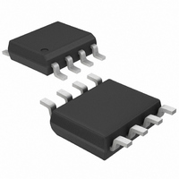
DS1302Z+ Maxim Integrated Products, DS1302Z+ Datasheet - Page 6

DS1302Z+
Manufacturer Part Number
DS1302Z+
Description
IC TIMEKEEPER W/CHARGER 8-SOIC
Manufacturer
Maxim Integrated Products
Type
Clock/Calendar/Trickle-Chargerr
Datasheet
1.DS1302ZTR.pdf
(13 pages)
Specifications of DS1302Z+
Memory Size
31B
Time Format
HH:MM:SS (12/24 hr)
Date Format
YY-MM-DD-dd
Interface
3-Wire Serial
Voltage - Supply
2 V ~ 5.5 V
Operating Temperature
0°C ~ 70°C
Mounting Type
Surface Mount
Package / Case
8-SOIC (3.9mm Width)
Function
Clock/Calendar/Trickle Charger/NV Timekeeping RAM
Rtc Memory Size
31 Byte
Supply Voltage (max)
5.5 V
Supply Voltage (min)
2 V
Maximum Operating Temperature
+ 70 C
Minimum Operating Temperature
0 C
Mounting Style
SMD/SMT
Rtc Bus Interface
Serial (3-Wire)
Supply Current
1.2 mA
Clock Format
HH
Clock Ic Type
RTC
Ic Interface Type
3 Wire
Memory Configuration
31 X 8
Supply Voltage Range
2V To 5.5V
Digital Ic Case Style
SOIC
No. Of Pins
8
Rohs Compliant
Yes
Lead Free Status / RoHS Status
Lead free / RoHS Compliant
DS1302 Trickle-Charge Timekeeping Chip
CE AND CLOCK CONTROL
Driving the CE input high initiates all data transfers. The CE input serves two functions. First, CE turns on the
control logic that allows access to the shift register for the address/command sequence. Second, the CE signal
provides a method of terminating either single-byte or multiple-byte CE data transfer.
A clock cycle is a sequence of a rising edge followed by a falling edge. For data inputs, data must be valid during
the rising edge of the clock and data bits are output on the falling edge of clock. If the CE input is low, all data
transfer terminates and the I/O pin goes to a high-impedance state. Figure 4 shows data transfer. At power-up, CE
must be a logic 0 until V
> 2.0V. Also, SCLK must be at a logic 0 when CE is driven to a logic 1 state.
CC
DATA INPUT
Following the eight SCLK cycles that input a write command byte, a data byte is input on the rising edge of the next
eight SCLK cycles. Additional SCLK cycles are ignored should they inadvertently occur. Data is input starting with
bit 0.
DATA OUTPUT
Following the eight SCLK cycles that input a read command byte, a data byte is output on the falling edge of the
next eight SCLK cycles. Note that the first data bit to be transmitted occurs on the first falling edge after the last bit
of the command byte is written. Additional SCLK cycles retransmit the data bytes should they inadvertently occur
so long as CE remains high. This operation permits continuous burst mode read capability. Also, the I/O pin is tri-
stated upon each rising edge of SCLK. Data is output starting with bit 0.
BURST MODE
Burst mode can be specified for either the clock/calendar or the RAM registers by addressing location 31 decimal
(address/command bits 1 through 5 = logic 1). As before, bit 6 specifies clock or RAM and bit 0 specifies read or
write. There is no data storage capacity at locations 9 through 31 in the Clock/Calendar Registers or location 31 in
the RAM registers. Reads or writes in burst mode start with bit 0 of address 0.
When writing to the clock registers in the burst mode, the first eight registers must be written in order for the data to
be transferred. However, when writing to RAM in burst mode it is not necessary to write all 31 bytes for the data to
transfer. Each byte that is written to will be transferred to RAM regardless of whether all 31 bytes are written or not.
CLOCK/CALENDAR
The time and calendar information is obtained by reading the appropriate register bytes. Table 3 illustrates the RTC
registers. The time and calendar are set or initialized by writing the appropriate register bytes. The contents of the
time and calendar registers are in the binary-coded decimal (BCD) format.
The day-of-week register increments at midnight. Values that correspond to the day of week are user-defined but
must be sequential (i.e., if 1 equals Sunday, then 2 equals Monday, and so on.). Illogical time and date entries
result in undefined operation.
When reading or writing the time and date registers, secondary (user) buffers are used to prevent errors when the
internal registers update. When reading the time and date registers, the user buffers are synchronized to the
internal registers the rising edge of CE.
The countdown chain is reset whenever the seconds register is written. Write transfers occur on the falling edge of
CE. To avoid rollover issues, once the countdown chain is reset, the remaining time and date registers must be
written within 1 second.
The DS1302 can be run in either 12-hour or 24-hour mode. Bit 7 of the hours register is defined as the 12- or 24-
hour mode-select bit. When high, the 12-hour mode is selected. In the 12-hour mode, bit 5 is the AM/ PM bit with
logic high being PM. In the 24-hour mode, bit 5 is the second 10-hour bit (20–23 hours). The hours data must be
re-initialized whenever the 12/ 24 bit is changed.
6 of 13


