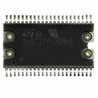
M48T37Y-70MH1E STMicroelectronics, M48T37Y-70MH1E Datasheet - Page 8

M48T37Y-70MH1E
Manufacturer Part Number
M48T37Y-70MH1E
Description
IC TIMEKPR NVRAM 256KBIT5V 44SOH
Manufacturer
STMicroelectronics
Series
Timekeeper®r
Type
Clock/Calendar/NVSRAMr
Specifications of M48T37Y-70MH1E
Memory Size
256K (32K x 8)
Time Format
HH:MM:SS (24 hr)
Date Format
YY-MM-DD-dd
Interface
Parallel
Voltage - Supply
4.5 V ~ 5.5 V
Operating Temperature
0°C ~ 70°C
Mounting Type
Surface Mount
Package / Case
44-SOH
Bus Type
Parallel
User Ram
32KB
Operating Supply Voltage (typ)
5V
Package Type
SOH
Operating Supply Voltage (max)
5.5V
Operating Supply Voltage (min)
4.5V
Operating Temperature Classification
Commercial
Operating Temperature (max)
70C
Operating Temperature (min)
0C
Pin Count
44
Mounting
Surface Mount
Memory Configuration
32K X 8
Nvram Features
RTC
Interface Type
Parallel
Access Time
70ns
Supply Voltage Range
4.5V To 5.5V
Memory Case Style
SOIC
No. Of Pins
44
Rohs Compliant
Yes
Lead Free Status / RoHS Status
Lead free / RoHS Compliant
Other names
497-2854-5
M48T37Y-70MH1
M48T37Y-70MH1
Available stocks
Company
Part Number
Manufacturer
Quantity
Price
Company:
Part Number:
M48T37Y-70MH1E
Manufacturer:
ST
Quantity:
936
M48T37Y, M48T37V
READ Mode
The M48T37Y/V is in the READ Mode whenever
WRITE Enable (W) is high and Chip Enable (E) is
low. The unique address specified by the 15 Ad-
dress Inputs defines which one of the 32,752 bytes
of data is to be accessed. Valid data will be avail-
able at the Data I/O pins within Address Access
time (t
stable, providing that the E and Output Enable (G)
access times are also satisfied. If the E and G ac-
cess times are not met, valid data will be available
Figure 5. READ Mode AC Waveforms
Note: WRITE Enable (W) = High.
Table 3. READ Mode AC Characteristics
Note: 1. Valid for Ambient Operating Temperature: T
8/29
Symbol
t
t
t
t
GLQX
EHQZ
GHQZ
ELQX
t
t
t
t
t
GLQV
AXQX
AVQV
ELQV
AVAV
2. C
AVQV
(2)
(2)
(2)
(2)
L
= 5pF.
A0-A14
E
G
DQ0-DQ7
) after the last address input signal is
READ Cycle Time
Address Valid to Output Valid
Chip Enable Low to Output Valid
Output Enable Low to Output Valid
Chip Enable Low to Output Transition
Output Enable Low to Output Transition
Chip Enable High to Output Hi-Z
Output Enable High to Output Hi-Z
Address Transition to Output Transition
Parameter
(1)
tAVQV
tELQX
tGLQX
tELQV
A
= 0 to 70°C or –40 to 85°C; V
tGLQV
tAVAV
VALID
after the latter of the Chip Enable Access time
(t
The state of the eight three-state Data I/O signals
is controlled by E and G. If the outputs are activat-
ed before t
indeterminate state until t
If the Address Inputs are changed while E and G
remain active, output data will remain valid for Out-
put Data Hold time (t
nate until the next Address Access.
Min
70
10
ELQV
5
5
M48T37Y
–70
) or Output Enable Access time (t
CC
AVQV
Max
= 4.5 to 5.5V or 3.0 to 3.6V (except where noted).
70
70
35
25
25
VALID
, the data lines will be driven to an
tGHQZ
AXQX
Min
100
10
10
5
M48T37V
AVQV
) but will be indetermi-
–100
.
Max
100
100
50
50
40
tAXQX
tEHQZ
AI00925
GLQV
Unit
ns
ns
ns
ns
ns
ns
ns
ns
ns
).


