PCA2125TS/1,112 NXP Semiconductors, PCA2125TS/1,112 Datasheet
PCA2125TS/1,112
Specifications of PCA2125TS/1,112
PCA2125TS/1
PCA2125TS/1


Related parts for PCA2125TS/1,112


PCA2125TS/1,112 Summary of contents
Page 1
PCA2125 SPI Real-time clock/calendar Rev. 01 — 28 July 2008 1. General description The PCA2125 is a CMOS real-time clock/calendar optimized for low-power consumption and an operating temperature up to 125 C. Data is transferred via a Serial Peripheral Interface ...
Page 2
... NXP Semiconductors 5. Marking Table 2. Type number PCA2125TS 6. Block diagram OSCI OSCILLATOR 32.768 kHz OSCO MONITOR POWER-ON RESET WATCH- DOG SDO SDI SPI INTERFACE SCL CE PCA2125 Fig 1. Block diagram of PCA2125 PCA2125_1 Product data sheet Marking codes DIVIDER CONTROL 00h Control_1 01h Control_2 ...
Page 3
... NXP Semiconductors 7. Pinning information 7.1 Pinning Fig 2. 7.2 Pin description Table 3. Symbol OSCI OSCO n.c. INT SDO SDI SCL n.c. CLKOUT Functional description The PCA2125 contains sixteen 8-bit registers with an auto-incrementing address register, an on-chip 32.768 kHz oscillator with one integrated capacitor, a frequency divider which provides the source clock for the Real-Time Clock (RTC), a programmable clock output, and a 6 MHz SPI-bus ...
Page 4
... NXP Semiconductors • The first two registers at addresses 00h and 01h (Control_1 and Control_2) are used as control registers. • Registers at addresses 02h to 08h (Seconds, Minutes, Hours, Days, Weekdays, Months, Years) are used as counters for the clock function. Seconds, minutes, hours, days, months and years are all coded in Binary Coded Decimal (BCD) format. When one of the RTC registers is read the contents of all counters are frozen ...
Page 5
... NXP Semiconductors Ten’s place mode. [2] 8.2 Reset The PCA2125 includes an internal reset circuit which is active whenever the oscillator is stopped; see the oscillator pins OSCI or OSCO to ground. Fig 3. The oscillator is considered to be stopped during the time between power-up and stable crystal resonance; see on crystal type, temperature and supply voltage. Whenever an internal reset occurs, the reset fl ...
Page 6
... NXP Semiconductors Table 5. Bits labeled ‘-’ are not implemented and will return a ‘0’ when read. Bits labeled ‘X’ are undefined at power-up and unchanged by subsequent resets. Address 07h 08h 09h 0Ah 0Bh 0Ch 0Dh 0Eh 0Fh After reset, the following mode is entered: • ...
Page 7
... NXP Semiconductors 8.3 Control registers Table 6. Bit Table 7. Bit PCA2125_1 Product data sheet Control_1 register (address 00h) bit description Symbol Value Description EXT_TEST 0 normal mode 1 external clock test mode - 0 unused STOP 0 RTC source clock runs 1 RTC divider chain flip-flops are asynchronously set to logic 0 ...
Page 8
... NXP Semiconductors 8.4 Time and date function The majority of the registers are coded in the Binary Coded Decimal (BCD) format. BCD is used to simplify application use. An example is shown for register Minutes in Table 8. Minutes value (decimal Table 9. Bit Table 10. Bit Table 11. Bit 6 and 7 12 hour mode ...
Page 9
... NXP Semiconductors Table 12. Bit [1] The RTC compensates for leap years by adding a 29th day to February if the year counter contains a value which is exactly divisible by 4, including the year 00. Table 13. Bit Table 14. [1] Day Sunday Monday Tuesday Wednesday Thursday Friday Saturday [1] The weekday assignments can be re-defined by the user. ...
Page 10
... NXP Semiconductors Table 16. Month October November December Table 17. Bit Figure 6 Fig 6. 8.5 Alarm function When one or several alarm registers are loaded with a valid minute, hour, day or weekday value and its corresponding alarm enable not bit (AENx) is logic 0, then that information is compared with the current minute, hour, day and weekday value. ...
Page 11
... NXP Semiconductors Table 19. Bit hour mode hour mode Table 20. Bit Table 21. Bit PCA2125_1 Product data sheet Register Hour_alarm (address 0Ah) bit description Symbol Value Description AEN_H 0 hour alarm is enabled 1 hour alarm is disabled - 0 unused AMPM 0 indicates AM 1 indicates PM HOUR_ALARM this register holds the hour alarm value coded in BCD ...
Page 12
... NXP Semiconductors Fig 7. Generation of interrupts from the alarm function is described in 8.5.1 Alarm flag When all enabled comparisons first match, the alarm flag bit AF is set. Bit AF will remain set until cleared by software. Once bit AF has been cleared it will only be set again when the time increments once more to match the alarm condition ...
Page 13
... NXP Semiconductors To prevent the timer flags being overwritten while clearing bit AF, a logic AND is performed during a write access. The flag is reset by writing a logic 0 but its value is not affected by writing a logic 1. Table 22. Register Control_2 Table 23 bit TF are unaffected. Table 23. Register Control_2 8.6 Timer functions The countdown timer has four selectable source clocks allowing for countdown periods in the range from less than more than 4 hours. There are also two pre-defi ...
Page 14
... NXP Semiconductors seconds counter minutes counter a. INT and MSF when SI enabled (MSF flag not cleared after an interrupt) seconds counter minutes counter b. INT and MSF when only MI enabled Fig 9. Table 26. Minute interrupt (bit MI The minute and second flag (bit MSF) is set to logic 1 when either the seconds or the minutes counter increments according to the currently enabled interrupt. The fl ...
Page 15
... NXP Semiconductors Table 27. Minute interrupt (bit MI [1] In the case of bit and bit bit MSF will be cleared automatically after 1 second. 8.6.2 Countdown timer function The 8-bit countdown timer at address 0Fh is controlled by the timer control register at address 0Eh. The timer control register determines one of 4 source clock frequencies for the timer (4096 Hz, 64 Hz, 1 Hz, or Table 28 ...
Page 16
... Fig 10. General countdown timer behavior If a new value written before the end of the current timer period, then this value will take immediate effect. NXP Semiconductors does not recommend changing n without first disabling the counter (by setting bit TE = 0). The update asynchronous with the ...
Page 17
... NXP Semiconductors When reading the timer, the current countdown value is returned and not the initial value n. For accurate read back of the countdown value, the SPI-bus clock (SCL) must be operating at a frequency of at least twice the selected timer clock. Since it is not possible to freeze the countdown timer counter during read back recommended to read the register twice and check for consistent results ...
Page 18
... NXP Semiconductors SECONDS COUNTER MINUTES COUNTER from interface: clear MSF TE COUNTDOWN COUNTER from interface: from interface: When bits SI, MI, TIE and AIE are all disabled, pin INT will remain high-impedance. Fig 11. Interrupt scheme Remark: Note that the interrupts from the three groups are wired-OR, meaning they will mask one another ...
Page 19
... NXP Semiconductors (1) Indicates normal duration of INT pulse (bit TI_TP = 1). Fig 12. Example of shortening the INT pulse by clearing the MSF flag The timing shown for clearing bit MSF in interrupt mode i.e. when bit TI_TP = 0, where the pulse can be shortened by setting both bits MI and SI to logic 0. ...
Page 20
... NXP Semiconductors (1) Indicates normal duration of INT pulse (bit TI_TP = 1). Fig 13. Example of shortening the INT pulse by clearing the TF flag The timing shown for clearing bit TF in mode i.e. when bit TI_TP = 0, where the pulse can be shortened by setting bit TIE = 0. 8.7.3 Alarm interrupts Generation of interrupts from the alarm function is controlled via bit AIE ...
Page 21
... NXP Semiconductors 8.8 Clock output A programmable square wave is available at pin CLKOUT. Operation is controlled by control bits COF[2:0] in register CLKOUT_control (0Dh). Frequencies of 32.768 kHz (default) down can be generated for use as a system clock, microcontroller clock, input to a charge pump, or for calibration of the oscillator. ...
Page 22
... NXP Semiconductors 1. Set EXT_TEST test mode (register Control_1, bit EXT_TEST = 1). 2. Set STOP (register Control_1, bit STOP = 1). 3. Clear STOP (register Control_1, bit STOP = 0). 4. Set time registers to desired value. 5. Apply 32 clock pulses to pin CLKOUT. 6. Read time registers to see the first change. ...
Page 23
... NXP Semiconductors The first increment of the time circuits is between 0.499888 s and 0.500000 s after stop is released. The uncertainty is caused by prescaler bits F0 and F1 not being reset; see Table Table 36. Example: first increment of time circuits after stop release Bit STOP Prescaler bits [ Clock is running normally ...
Page 24
... NXP Semiconductors 8.11 3-line SPI Data transfer to and from the device is made via a 3-wire SPI-bus; see lines for input and output are split. The data input and output lines can be connected together to facilitate a bidirectional data bus. The chip enable signal is used to identify the transmitted data. Each data transfer is a byte, with the Most Signifi ...
Page 25
... NXP Semiconductors R SCL SDI CE address xx counter Fig 19. Serial bus write example In Figure 20 are not connected together. In this configuration important that pin SDI is never left floating: it must always be driven either HIGH or LOW. If pin SDI is left open, high I currents will result. R/W ...
Page 26
... NXP Semiconductors 9. Internal circuitry Fig 21. Device diode protection diagram 10. Limiting values Table 39. In accordance with the Absolute Maximum Rating System (IEC 60134). Symbol Parameter tot T amb T stg V esd I lu [1] HBM: Human Body Model, according to JESD22-A114. [2] MM: Machine Model, according to JESD22-A115. [3] CDM: Charged-Device Model, according to JESD22-C101. ...
Page 27
... NXP Semiconductors 11. Static characteristics Table 40. Static characteristics otherwise specified. Symbol Parameter Supply: pin supply voltage DD I supply current DD Inputs V input voltage I V input voltage I V LOW-level input voltage IL V HIGH-level input voltage IH I leakage current L C input capacitance I R pull-down resistance ...
Page 28
... NXP Semiconductors Table 40. Static characteristics otherwise specified. Symbol Parameter I HIGH-level output current OH I LOW-level output current OL I LOW-level output current OL I output leakage current LO C external capacitance ext [1] For reliable oscillator start at power-up [2] Timer source clock = Hz; voltage on pins CE, SDI and SCL at V ...
Page 29
... NXP Semiconductors CE t su(CE) SCL WRITE SDI R/W SA2 Hi Z SDO READ SDI SDO Fig 22. SPI interface timing PCA2125_1 Product data sheet t w(CE 80% 20% RA0 t(SDI-SDO) t d(R)SDO b7 b6 Rev. 01 — 28 July 2008 PCA2125 SPI Real-time clock/calendar t h(CE) t clk(L) t clk( dis(SDO) b0 001aag900 © ...
Page 30
... NXP Semiconductors 13. Application information 13.1 Application diagram Fig 23. Application diagram 13.2 Quartz frequency adjustment 1. Method 1: fixed OSCI capacitor A fixed capacitor can be used whose value can be determined by evaluating the average capacitance necessary for the application layout; see frequency is best measured via the 32.768 kHz signal at pin CLKOUT available after power-on ...
Page 31
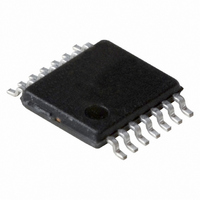
... NXP Semiconductors 15. Package outline TSSOP14: plastic thin shrink small outline package; 14 leads; body width 4 pin 1 index 1 e DIMENSIONS (mm are the original dimensions) A UNIT max. 0.15 0.95 mm 1.1 0.25 0.05 0.80 Notes 1. Plastic or metal protrusions of 0.15 mm maximum per side are not included. ...
Page 32
... NXP Semiconductors 16. Handling information Inputs and outputs are protected against electrostatic discharge in normal handling. However completely safe you must take normal precautions appropriate to handling MOS devices; see JESD625-A and/or IEC61340-5 . 17. Soldering of SMD packages This text provides a very brief insight into a complex technology. A more in-depth account of soldering ICs can be found in Application Note AN10365 “ ...
Page 33
... NXP Semiconductors • Process issues, such as application of adhesive and flux, clinching of leads, board transport, the solder wave parameters, and the time during which components are exposed to the wave • Solder bath specifications, including temperature and impurities 17.4 Reflow soldering Key characteristics in reflow soldering are: • ...
Page 34
... NXP Semiconductors Fig 25. Temperature profiles for large and small components For further information on temperature profiles, refer to Application Note AN10365 “Surface mount reflow soldering description” . 18. Revision history Table 44. Revision history Document ID Release date PCA2125_1 20080728 PCA2125_1 Product data sheet ...
Page 35
... Right to make changes — NXP Semiconductors reserves the right to make changes to information published in this document, including without limitation specifications and product descriptions, at any time and without notice ...
Page 36
... NXP Semiconductors 22. Contents 1 General description . . . . . . . . . . . . . . . . . . . . . . 1 2 Features . . . . . . . . . . . . . . . . . . . . . . . . . . . . . . . 1 3 Applications . . . . . . . . . . . . . . . . . . . . . . . . . . . . 1 4 Ordering information . . . . . . . . . . . . . . . . . . . . . 1 5 Marking . . . . . . . . . . . . . . . . . . . . . . . . . . . . . . . . 2 6 Block diagram . . . . . . . . . . . . . . . . . . . . . . . . . . 2 7 Pinning information . . . . . . . . . . . . . . . . . . . . . . 3 7.1 Pinning . . . . . . . . . . . . . . . . . . . . . . . . . . . . . . . 3 7.2 Pin description . . . . . . . . . . . . . . . . . . . . . . . . . 3 8 Functional description . . . . . . . . . . . . . . . . . . . 3 8.1 Register overview . . . . . . . . . . . . . . . . . . . . . . . 4 8.2 Reset . . . . . . . . . . . . . . . . . . . . . . . . . . . . . . . . 5 8.2.1 Power-on reset override . . . . . . . . . . . . . . . . . . 6 8.3 Control registers . . . . . . . . . . . . . . . . . . . . . . . . 7 8.4 Time and date function ...