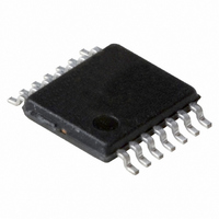
PCA2125TS/1,112 NXP Semiconductors, PCA2125TS/1,112 Datasheet - Page 28

PCA2125TS/1,112
Manufacturer Part Number
PCA2125TS/1,112
Description
IC CMOS RTC/CALENDAR 14-TSSOP
Manufacturer
NXP Semiconductors
Type
Clock/Calendar/Alarmr
Datasheet
1.PCA2125TS1112.pdf
(36 pages)
Specifications of PCA2125TS/1,112
Package / Case
14-TSSOP
Time Format
HH:MM:SS (12/24 hr)
Date Format
YY-MM-DD-dd
Interface
SPI, 3-Wire Serial
Voltage - Supply
1.3 V ~ 5.5 V
Operating Temperature
-40°C ~ 125°C
Mounting Type
Surface Mount
Function
Clock, Calendar
Supply Voltage (max)
5.5 V
Supply Voltage (min)
1.3 V
Maximum Operating Temperature
+ 125 C
Minimum Operating Temperature
- 40 C
Mounting Style
SMD/SMT
Rtc Bus Interface
Serial
Lead Free Status / RoHS Status
Lead free / RoHS Compliant
For Use With
OM6292 - DEMO BOARD PCA2125 RTC
Memory Size
-
Lead Free Status / RoHS Status
Lead free / RoHS Compliant, Lead free / RoHS Compliant
Other names
935283386112
PCA2125TS/1
PCA2125TS/1
PCA2125TS/1
PCA2125TS/1
NXP Semiconductors
Table 40.
V
otherwise specified.
[1]
[2]
[3]
12. Dynamic characteristics
Table 41.
V
All timing values are valid within the operating supply voltage at ambient temperature and referenced to V
input voltage swing of V
[1]
PCA2125_1
Product data sheet
Symbol
I
I
I
I
C
Symbol
Pin SCL
f
t
t
t
t
t
Pin CE
t
t
t
t
Pin SDI
t
t
Pin SDO
t
t
t
OH
OL
OL
LO
clk(SCL)
SCL
clk(H)
clk(L)
r
f
su(CE)
h(CE)
rec(CE)
w(CE)
su
h
d(R)SDO
dis(SDO)
t(SDI-SDO)
DD
DD
ext
= 1.3 V to 5.5 V; V
For reliable oscillator start at power-up: V
Timer source clock =
Implicit by design.
= 1.6 V to 5.5 V; V
Bus will be held up by bus capacitance; use RC time constant with application values.
Parameter
HIGH-level output current
LOW-level output current
LOW-level output current
output leakage current
external capacitance
Parameter
SCL clock frequency
SCL time
clock HIGH time
clock LOW time
rise time
fall time
CE set-up time
CE hold time
CE recovery time
CE pulse width
set-up time
hold time
SDO read delay time bus load = 85 pF
SDO disable time
transition time from
SDI to SDO
Static characteristics
Dynamic characteristics
SS
SS
1
SS
60
= 0 V; T
= 0 V; T
to V
Hz; voltage on pins CE, SDI and SCL at V
DD
.
amb
amb
Conditions
no load value
to avoid bus conflict
…continued
= 40 C to +125 C; f
= 40 C to +125 C.
DD
Conditions
pin SDO; V
pins INT, SDO and CLKOUT;
V
pin OSCO; V
V
OL
O
= V
= V
= 0.4 V; V
DD(min)
DD
Rev. 01 — 28 July 2008
or V
+ 0.3 V.
OH
OL
SS
DD
= 4.6 V; V
[1]
= 0.4 V; V
= 5 V
osc
V
Min
660
320
320
100
100
100
30
25
DD
0
= 32.768 kHz; quartz R
-
-
-
-
-
-
DD
= 1.6 V
DD
or V
DD
Max
0.99
100
100
320
1.5
= 5 V
50
-
-
-
-
-
-
-
-
-
= 5 V
SS
.
V
Min
210
100
110
100
30
60
15
60
DD
0
-
-
-
-
-
-
= 2.7 V
Min
-
-
Max
4.76
0.99
100
100
110
1.5
1
1
30
-
-
-
-
-
-
-
-
-
s
= 60 k ; C
V
SPI Real-time clock/calendar
Min
200
100
100
100
30
40
15
40
DD
0
-
-
-
-
-
-
Typ
-
-
-
0
25
= 4.5 V
Max
5.00
0.99
100
100
100
30
L
-
-
-
-
-
-
-
-
-
= 12.5 pF; unless
PCA2125
© NXP B.V. 2008. All rights reserved.
V
Max
1.5
-
-
+1
-
Min
160
100
IL
70
90
30
30
10
30
DD
0
-
-
-
-
-
-
and V
= 5.5 V Unit
Max
6.25 MHz
0.99 s
100
100
90
25
IH
-
-
-
-
-
-
-
-
-
with an
Unit
mA
mA
mA
pF
28 of 36
A
ns
ns
ns
ns
ns
ns
ns
ns
ns
ns
ns
ns
ns


