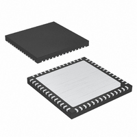
MAX19713ETN+ Maxim Integrated Products, MAX19713ETN+ Datasheet - Page 17

MAX19713ETN+
Manufacturer Part Number
MAX19713ETN+
Description
IC ANLG FRONT END 45MSPS 56-TQFN
Manufacturer
Maxim Integrated Products
Datasheet
1.MAX19713ETN.pdf
(37 pages)
Specifications of MAX19713ETN+
Number Of Bits
10
Number Of Channels
2
Power (watts)
91.8mW
Voltage - Supply, Analog
3V
Voltage - Supply, Digital
3V
Package / Case
56-TQFN Exposed Pad
Lead Free Status / RoHS Status
Lead free / RoHS Compliant
IAN, as well as QAP and QAN, and set the input signal
common-mode voltage within the V
ADC range for optimum performance.
Figure 3 shows the relationship between the clock, ana-
log inputs, and the resulting output data. Channels IA
and QA are sampled on the rising edge of the clock sig-
nal (CLK) and the resulting data is multiplexed at the
AD0–AD9 outputs. Channel IA data is updated on the ris-
ing edge and channel QA data is updated on the falling
Table 1. Rx ADC Output Codes vs. Input Voltage
Figure 2. Rx ADC Transfer Function
DIFFERENTIAL INPUT
11 1111 1111
11 1111 1110
11 1111 1101
10 0000 0001
10 0000 0000
01 1111 1111
00 0000 0011
00 0000 0010
00 0000 0001
00 0000 0000
-V
-V
V
V
-V
V
V
REF
REF
REF
REF
VOLTAGE
REF
REF
REF
x 512/512
x 511/512
x 511/512
x 512/512
x 1/512
x 0/512
x 1/512
-512
Rx ADC System Timing Requirements
-511
1 LSB =
______________________________________________________________________________________
-510 -509
2 x V
V
REF
1024
REF
INPUT VOLTAGE (LSB)
-1
(COM)
DIFFERENTIAL INPUT (LSB)
0+ 1
-511 (-Full Scale + 1 LSB)
511 (+Full Scale - 1 LSB)
510 (+Full Scale - 2 LSB)
V
REF
-512 (-Full Scale)
DD
0 (Bipolar Zero)
V
= V
REF
REFP
+509
/ 2 (±0.8V) Rx
+510
- V
+1
-1
REFN
+511
+512
(COM)
10-Bit, 45Msps, Full-Duplex
OFFSET BINARY (AD0–AD9)
edge of CLK. Including the delay through the output
latch, the total clock-cycle latency is 5 clock cycles for
channel IA and 5.5 clock cycles for channel QA.
AD0–AD9 are the Rx ADC digital logic outputs of the
MAX19713. The logic level is set by OV
V
Keep the capacitive load on the digital outputs AD0–AD9
as low as possible (< 15pF) to avoid large digital currents
feeding back into the analog portion of the MAX19713
and degrading its dynamic performance. Buffers on the
digital outputs isolate the outputs from heavy capacitive
loads. Adding 100Ω resistors in series with the digital out-
puts close to the MAX19713 will help improve ADC per-
formance. Refer to the MAX19713EVKIT schematic for an
example of the digital outputs driving a digital buffer
through 100Ω series resistors.
During SHDN, IDLE, STBY, SPI2, and SPI4 states, digital
outputs AD0–AD9 are tri-stated.
The dual 10-bit digital-to-analog converters (Tx DACs)
operate with clock speeds up to 45MHz. The Tx DAC
digital inputs, DA0–DA9, are multiplexed on a single
10-bit transmit bus. The voltage reference determines
the Tx DAC full-scale voltage at IDP, IDN and QDP,
QDN analog outputs. See the Reference Configurations
section for setting the reference voltage.
DD
. The digital output coding is offset binary (Table 1).
11 1111 1111
11 1111 1110
10 0000 0001
10 0000 0000
01 1111 1111
00 0000 0001
00 0000 0000
Analog Front-End
Digital Output Data (AD0–AD9)
OUTPUT DECIMAL CODE
Dual 10-Bit Tx DACs
1023
1022
513
512
511
DD
1
0
from 1.8V to
17


