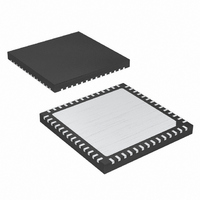
MAX19713ETN+ Maxim Integrated Products, MAX19713ETN+ Datasheet - Page 26

MAX19713ETN+
Manufacturer Part Number
MAX19713ETN+
Description
IC ANLG FRONT END 45MSPS 56-TQFN
Manufacturer
Maxim Integrated Products
Datasheet
1.MAX19713ETN.pdf
(37 pages)
Specifications of MAX19713ETN+
Number Of Bits
10
Number Of Channels
2
Power (watts)
91.8mW
Voltage - Supply, Analog
3V
Voltage - Supply, Digital
3V
Package / Case
56-TQFN Exposed Pad
Lead Free Status / RoHS Status
Lead free / RoHS Compliant
Both the Rx ADC and Tx DAC share the CLK input. The
CLK input accepts a CMOS-compatible signal level set
by OV
version of the device depends on the repeatability of
the rising and falling edges of the external clock, use a
clock with low jitter and fast rise and fall times (< 2ns).
Specifically, sampling occurs on the rising edge of the
clock signal, requiring this edge to provide the lowest
possible jitter. Any significant clock jitter limits the SNR
performance of the on-chip Rx ADC as follows:
where f
t
Clock jitter is especially critical for undersampling
applications. Consider the clock input as an analog
input and route away from any analog input or other
digital signal lines. The MAX19713 clock input operates
with an OV
±10% duty cycle.
When the clock signal is stopped at CLK input (CLK =
0 or OV
and the MAX19713 saves the last power-management
mode or Tx/Rx/FD command. All converter circuits (Rx
ADC, Tx DAC, aux-ADC, and aux-DACs) hold their last
value. When the clock signal is restarted at CLK, allow
3.8µs (clock wake-up time) for the internal clock circuit-
ry to settle before updating the Tx DAC, reading a valid
Rx ADC conversion result, or starting an aux-ADC con-
version. This ensures the converters (Rx ADC, Tx DAC,
aux-ADC) meet all dynamic performance specifica-
tions. The aux-DAC channels are not dependent on
CLK, so they can be updated when CLK is idle.
The MAX19713 includes three 12-bit aux-DACs (DAC1,
DAC2, DAC3) with 1µs settling time for controlling vari-
able-gain amplifier (VGA), automatic gain-control
(AGC), and automatic frequency-control (AFC) func-
tions. The aux-DAC output range is 0.2V to 2.57V as
defined by V
AGC outputs (DAC2 and DAC3) are at zero. The AFC
DAC (DAC1) is at 1.1V during power-up. The aux-DACs
can be independently controlled through the SPI bus,
except during SHDN mode where the aux-DACs are
turned off completely and the output voltage is set to
zero. In STBY and IDLE modes the aux-DACs maintain
the last value. On wake-up from SHDN, the aux-DACs
resume the last values.
10-Bit, 45Msps, Full-Duplex
Analog Front-End
26
AJ
is the time of the clock jitter.
______________________________________________________________________________________
DD
IN
DD
SNR
from 1.8V to V
represents the analog input frequency and
DD
), all internal registers hold their last value
OH
=
/ 2 voltage threshold and accepts a 50%
20
- V
12-Bit, Auxiliary Control DACs
×
OL
log
System Clock Input (CLK)
. During power-up, the VGA and
⎛
⎜
⎝
2
DD
×
. Since the interstage con-
π
×
1
f
IN
×
t
AJ
⎞
⎟
⎠
Loading on the aux-DAC outputs should be carefully
observed to achieve the specified settling time and sta-
bility. The capacitive load must be kept to a maximum
of 5pF including package and trace capacitance. The
resistive load must be greater than 200kΩ. If capacitive
loading exceeds 5pF, then add a 10kΩ resistor in
series with the output. Adding the series resistor helps
drive larger load capacitance (< 15pF) at the expense
of slower settling time.
The MAX19713 integrates a 333ksps, 10-bit aux-ADC
with an input 4:1 multiplexer. In the aux-ADC mode reg-
ister, setting bit AD0 begins a conversion with the auxil-
iary ADC. Bit AD0 automatically clears when the
conversion is complete. Setting or clearing AD0 during
a conversion has no effect (see Table 12). Bit AD1
determines the internal reference of the auxiliary ADC
(see Table 13). Bits AD2 and AD3 determine the auxil-
iary ADC input source (see Table 14). Bits AD4, AD5,
and AD6 select the number of averages taken when a
single start-convert command is given. The conversion
time increases as the number of averages increases
(see Table 15). The conversion clock can be divided
down from the system clock by properly setting bits
AD7, AD8, and AD9 (see Table 16). The aux-ADC out-
put data can be written out of DOUT by setting bit
AD10 high (see Table 17).
The aux-ADC features a 4:1 input multiplexer to allow
measurements on four input sources. The input sources
are selected by AD3 and AD2 (see Table 14). Two of
the multiplexer inputs (ADC1 and ADC2) can be con-
nected to external sources such as an RF power detec-
tor like the MAX2208 or temperature sensor like the
MAX6613. The other two multiplexer inputs are internal
connections to V
supply voltages. The internal V
tions are made through integrated dividers that yield
V
ADC voltage reference can be selected between an
internal 2.048V bandgap reference or V
13). The V
measurement of an external voltage source with a full-
scale range extending beyond the 2.048V level. The
input source voltage range cannot extend above V
The conversion requires 12 clock edges (1 for input
sampling, 1 for each of the 10 bits, and 1 at the end for
loading into the serial output register) to complete one
conversion cycle (when no averaging is being done).
Each conversion of an average (when averaging is set
greater than 1) requires 12 clock edges. The conver-
sion clock is generated from the system clock input
(CLK). An SPI-programmable divider divides the system
DD
/ 2 and OV
DD
reference selection is provided to allow
DD
10-Bit, 333ksps Auxiliary ADC
DD
/ 2 measurement results. The aux-
and OV
DD
that monitor the power-
DD
and OV
DD
DD
(see Table
connec-
DD
.


