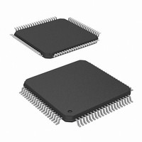
ISL98003INZ-110 Intersil, ISL98003INZ-110 Datasheet - Page 25

ISL98003INZ-110
Manufacturer Part Number
ISL98003INZ-110
Description
IC AFE 3CH 8BIT 110MHZ 80EPTQFP
Manufacturer
Intersil
Datasheet
1.ISL98003CNZ-110.pdf
(31 pages)
Specifications of ISL98003INZ-110
Number Of Bits
8
Number Of Channels
3
Power (watts)
1.1W
Voltage - Supply, Analog
1.8V, 3.3V
Voltage - Supply, Digital
1.65 V ~ 2 V
Package / Case
80-TQFP Exposed Pad, 80-eTQFP, 80-HTQFP, 80-VQFP
Lead Free Status / RoHS Status
Lead free / RoHS Compliant
Available stocks
Company
Part Number
Manufacturer
Quantity
Price
Company:
Part Number:
ISL98003INZ-110
Manufacturer:
GE
Quantity:
340
The default Offset DAC range is ±127 ADC LSBs. Setting
0x27[1] = 1 reduces the swing of the Offset DAC by 50%,
making 1 Offset DAC LSB the weight of 1/8 of an ADC LSB.
This provides the finest offset control and applies to both
ABLC™ and manual modes.
Automatic Black Level Compensation (ABLC)
ABLC is a function that continuously removes all offset
errors from the incoming video signal by monitoring the
offset at the output of the ADC and servoing the 10-bit
analog DAC to force those errors to zero. When ABLC is
enabled, the user offset control is a digital adder, with 8-bit
resolution.
When the ABLC function is enabled (0x27[0] = 0), the ABLC
function is executed every line after the trailing edge of
HSYNC. If register 0x60[2] = 0 (the default), the ABLC
function will be not be triggered while the DPLL is coasting,
preventing any composite sync edges, equalization pulses,
or Macrovision signals from corrupting the black data and
potentially adding a small error in the ABLC accumulator.
After the trailing edge of HSYNC, the start of ABLC is
delayed by the number of pixels specified in registers 0x24
and 0x25. After that delay, the number of pixels specified
by register 0x27[3:2] are averaged together and added to
the ABLC’s accumulator. The accumulator stores the
average black levels for the number of lines specified by
register 0x27[6:4], which is then used to generate a 10-bit
DAC value.
The ABLC can be set to allow the capture of signals below
black by setting registers 0x65, 0x66 and 0x67 to a number
that will control the target for the ABLC servo loop. If you set
register 0x65 to 0x10 then the ABLC will adjust the offset
DAC to produce an average output code on the Red channel
of 0x10 during the back porch. Effectively, the black level for
a given channel will be set to the value of its ABLC offset
target register (output = register 0x65, 0x66 or 0x67).
ADC
The ISL98003 features 3 fully differential, high-speed 8-bit
ADCs.
Clock Generation
A Digital Phase Lock Loop (DPLL) is employed to generate
the pixel clock frequency. The HSYNC input and the external
XTAL provide a reference frequency to the PLL. The PLL
then generates the pixel clock frequency that equal to the
incoming HSYNC frequency times the HTOTAL value
programmed into registers 0x1E and 0x1F.
The stability of the clock is very important and correlates
directly with the quality of the image. During each pixel time
transition, there is a small window where the signal is
slewing from the old pixel amplitude and settling to the new
pixel value. At higher frequencies, the pixel time transitions
at a faster rate, which makes the stable pixel time even
smaller. Any jitter in the pixel clock reduces the effective
25
ISL98003
stable pixel time and thus the sample window in which pixel
sampling can be made accurately.
Sampling Phase
The ISL98003 provides 64 low-jitter phase choices per pixel
period, allowing the firmware to precisely select the optimum
sampling point. The sampling phase register is 0x20.
Auto Phase Adjust
The ISL98003 provides the ability to automatically adjust the
Sampling Phase to the best setting. Set register 0x50 to
0x03 to activate the auto phase adjust function.
Data Enable (DE) Generator
The ISL98003 provides a signal that is high during the active
video time when properly configured. This signal is used by
devices such as DVI/HDMI transmitters to gate the active
portion of the video and ignore the H and V sync times.
Auto DE Adjust
The ISL98003 provides the ability to automatically adjust the
DE to the settings that are very close to ideal. The
determination of exactly where on a line the active video
starts and ends depends heavily on the video content being
analyzed making the DE settings difficult to automate. The
customer will be required to fine tune the DE settings after
the Auto Adjust routine has completed. Set register 0x50 to
0x04 to activate the auto DE adjust function
HSYNC Slicer
To further minimize jitter, the HSYNC inputs are treated as
analog signals, and brought into a precision slicer block with
thresholds programmable in 400mV steps with 240mV of
hysteresis, and a subsequent digital glitch filter that ignores
any HSYNC transitions within 100ns of the initial transition.
This processing greatly increases the AFE’s rejection of
ringing and reflections on the HSYNC line and allows the
AFE to perform well even with pathological HSYNC signals.
Voltages given above and in the HSYNC Slicer register
description are with respect to a 3.3V sync signal at the
HSYNC
resistor should be placed between the HSYNC source and the
HSYNC
between the HSYNC
input, the hysteresis will be 240mV*5V/3.3V = 360mV, and the
slicer step size will be 400mV*5V/3.3V = 600mV per step.
SYNC Status and Polarity Detection
The CH0 and CH1 Activity Status register (0x02)
continuously monitors all 6 sync inputs (VSYNC
HSYNC
their status while the Selected Input Channel Characteristics
register (0x01) gives more detailed information on the
currently selected input channel.
However, accurate sync activity detection is always a
challenge. Noise and repetitive video patterns on the Green
IN
IN
IN
, and SOG
input pin. To achieve 5V compatibility, a 1kΩ series
input pin and a 1.9kΩ resistor should be placed
IN
IN
input pin and ground. Relative to a 5V
for both of the channels) and report
September 12, 2008
IN
,
FN6760.0


