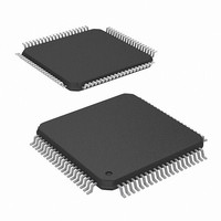
ISL98003INZ-110 Intersil, ISL98003INZ-110 Datasheet - Page 27

ISL98003INZ-110
Manufacturer Part Number
ISL98003INZ-110
Description
IC AFE 3CH 8BIT 110MHZ 80EPTQFP
Manufacturer
Intersil
Datasheet
1.ISL98003CNZ-110.pdf
(31 pages)
Specifications of ISL98003INZ-110
Number Of Bits
8
Number Of Channels
3
Power (watts)
1.1W
Voltage - Supply, Analog
1.8V, 3.3V
Voltage - Supply, Digital
1.65 V ~ 2 V
Package / Case
80-TQFP Exposed Pad, 80-eTQFP, 80-HTQFP, 80-VQFP
Lead Free Status / RoHS Status
Lead free / RoHS Compliant
Available stocks
Company
Part Number
Manufacturer
Quantity
Price
Company:
Part Number:
ISL98003INZ-110
Manufacturer:
GE
Quantity:
340
Crystal Oscillator
An external 12MHz to 27MHz crystal supplies the low-jitter
reference clock to the DPLL. The absolute frequency of this
crystal within this range is unimportant, as is the crystal’s
temperature coefficient, allowing use of less expensive,
lower-grade crystals.
As an alternative to a crystal, the XTAL
with a 3.3V CMOS-level external clock source at any
frequency between 12MHz and 27MHz. The ISL98003’s
jitter specification assumes a low-jitter crystal source. If the
external clock source has increased jitter, the sample clock
generated by the DPLL may exhibit increased jitter as well.
EMI Considerations
There are two possible sources of EMI on the ISL98003, as
follows.
CRYSTAL OSCILLATOR
The EMI from the crystal oscillator is negligible. This is due to
an amplitude-regulated, low voltage sine wave oscillator circuit,
instead of the typical high-gain square wave inverter-type
oscillator, so there are no harmonics. The crystal oscillator is
not a significant source of EMI.
DIGITAL OUTPUT SWITCHING
This is the largest potential source of EMI. However, the EMI is
determined by the PCB layout and the loading on the databus.
The way to control this is to put series resistors on the output of
all the digital pins (as our demo board and reference circuits
show). These resistors should be as large as possible, while
still meeting the setup and hold timing requirements of the
scaler. We recommend starting with 22Ω. If the databus is
heavily loaded (long traces, many other part on the same bus),
this value may need to be reduced. If the databus is lightly
loaded, it may be increased.
Intersil’s recommendations to minimize EMI are:
• Minimize the databus trace length
• Minimize the databus capacitive loading.
If EMI is a problem in the final design, increase the value of the
digital output series resistors to reduce slew rates on the bus.
This can only be done as long as the scaler’s setup and hold
timing requirements continue to be met.
Standby Mode
The ISL98003 can be placed into a low power standby mode
by writing a 0x0F to register 0x2C, powering down the triple
ADCs, the DPLL, and most of the internal clocks.
To allow input monitoring and mode detection during
power-down, the following blocks remain active:
• Serial interface (including the crystal oscillator) to enable
• Activity and polarity detect functions (registers 0x01 and
register read/write activity
27
IN
pin can be driven
ISL98003
• The HSYNC
Initialization
The ISL98003 initializes with default register settings for an
AC-coupled, RGB input on the VGA1 channel.
Reset
The ISL98003 has a Power On Reset (POR) function that
resets the chip to its default state when power is initially
applied, including resetting all the registers to their default
settings as described in the “Register Listing” on page 10.
The POR function takes 512k Crystal clocks (~21ms at
25MHz) to complete. The external RESET pin duplicates the
reset function of the POR without having to cycle the power
supplies. The RESET pin does not need to be used in
normal operation and can be tied high.
ISL98003 Serial Communication
Overview
The ISL98003 uses a 2-wire serial bus for communication
with its host. SCL is the Serial Clock line, driven by the host,
and SDA is the Serial Data line, which can be driven by all
devices on the bus. SDA is open drain to allow multiple
devices to share the same bus simultaneously.
Communication is accomplished in three steps:
The ISL98003 has a 7-bit address (1001100) on the serial
bus.
The bus is nominally inactive, with SDA and SCL high.
Communication begins when the host issues a START
command by taking SDA low while SCL is high (Figure 3).
The ISL98003 continuously monitors the SDA and SCL lines
for the start condition and will not respond to any command
until this condition has been met. The host then transmits the
7-bit serial address plus a R/W bit, indicating if the next
transaction will be a Read (R/W = 1) or a Write (R/W = 0). If
the address transmitted matches that of any device on the
bus, that device must respond with an ACKNOWLEDGE
(see Figure 4).
1. The Host selects the ISL98003 it wishes to communicate
2. The Host writes the initial ISL98003 Configuration
3. The Host writes to or reads from the ISL98003’s
0x02)
with.
Register address it wishes to write to or read from.
Configuration Register. The ISL98003’s internal address
pointer auto increments, so to read registers 0x00
through 0x1B, for example, one would write 0x00 in
Step 2, then repeat Step 3 (28) times, with each read
returning the next register value.
OUT
and VSYNC
OUT
pins (for mode detection)
September 12, 2008
FN6760.0


