ADC108S052CIMT/NOPB National Semiconductor, ADC108S052CIMT/NOPB Datasheet
ADC108S052CIMT/NOPB
Specifications of ADC108S052CIMT/NOPB
*ADC108S052CIMT/NOPB
ADC108S052CIMT


Related parts for ADC108S052CIMT/NOPB

ADC108S052CIMT/NOPB Summary of contents
Page 1
... Operation over the extended industrial temperature range of −40°C to +105°C is guaranteed. Connection Diagram Ordering Information Order Code ADC108S052CIMT ADC108S052CIMTX ADC108S052EVAL SPI ™ trademark of Motorola, Inc. © 2011 National Semiconductor Corporation ADC108S052 Features ■ Eight input channels ■ Variable power management ■ Independent analog and digital supplies ■ ...
Page 2
Block Diagram Pin Descriptions and Equivalent Circuits Pin No. Symbol ANALOG I/O IN0 to IN7 DIGITAL I/O 16 SCLK 15 DOUT 14 DIN 1 CS POWER SUPPLY AGND 12 DGND ...
Page 3
... Absolute Maximum Ratings If Military/Aerospace specified devices are required, please contact the National Semiconductor Sales Office/ Distributors for availability and specifications. Analog Supply Voltage V A Digital Supply Voltage V D Voltage on Any Pin to GND Input Current at Any Pin (Note 3) Package Input Current(Note 3) Power Dissipation 25° ...
Page 4
Symbol Parameter DIGITAL INPUT CHARACTERISTICS V Input High Voltage IH V Input Low Voltage IL I Input Current IN C Digital Input Capacitance IND DIGITAL OUTPUT CHARACTERISTICS V Output High Voltage OH V Output Low Voltage ...
Page 5
ADC108S052 Timing Specifications The following specifications apply for V ksps to 500 ksps, and C = 50pF. Boldface limits apply for T L Symbol Parameter t CS Hold Time after SCLK Rising Edge CSH CS Setup Time prior to SCLK ...
Page 6
Timing Diagrams www.national.com FIGURE 1. ADC108S052 Operational Timing Diagram FIGURE 2. ADC108S052 Serial Timing Diagram FIGURE 3. SCLK and CS Timing Parameters 6 20164451 20164406 20164450 ...
Page 7
Specification Definitions ACQUISITION TIME is the time required for the ADC to ac- quire the input voltage. During this time, the hold capacitor is charged by the input voltage. APERTURE DELAY is the time between the fourth falling edge of ...
Page 8
Typical Performance Characteristics unless otherwise stated. DNL INL DNL vs. Supply www.national.com T = +25° 500 ksps SAMPLE 20164440 20164442 INL vs. Supply 20164421 MHz 40.2 kHz SCLK IN DNL 20164441 ...
Page 9
SNR vs. Supply 20164422 ENOB vs. Supply 20164433 INL vs. V with 20164431 THD vs. Supply DNL vs. V with DNL vs. SCLK Duty Cycle 9 20164432 = 5.0 V 20164430 ...
Page 10
INL vs. SCLK Duty Cycle THD vs. SCLK Duty Cycle DNL vs. SCLK www.national.com SNR vs. SCLK Duty Cycle 20164458 ENOB vs. SCLK Duty Cycle 20164464 20164456 10 20164461 20164452 INL vs. SCLK 20164459 ...
Page 11
SNR vs. SCLK 20164462 ENOB vs. SCLK 20164453 INL vs. Temperature 20164460 THD vs. SCLK DNL vs. Temperature SNR vs. Temperature 11 20164465 20164457 20164463 www.national.com ...
Page 12
THD vs. Temperature SNR vs. Input Frequency ENOB vs. Input Frequency www.national.com ENOB vs. Temperature 20164466 THD vs. Input Frequency 20164423 Power Consumption vs. SCLK 20164425 12 20164454 20164424 20164444 ...
Page 13
Functional Description The ADC108S052 is a successive-approximation analog-to- digital converter designed around a charge-redistribution dig- ital-to-analog converter. 1.1 ADC108S052 OPERATION Simplified schematics of the ADC108S052 in both track and hold operation are shown in Figure 4 and tively. In ...
Page 14
ADC enters track mode. While there is no timing restriction with respect to the rising edges of CS and SCLK, see 3 for setup and hold time requirements for the falling edge of CS with respect to the rising ...
Page 15
Applications Information 2.1 TYPICAL APPLICATION CIRCUIT A typical application is shown in Figure 8. The split analog and digital supply pins are both powered in this example by the National LP2950 low-dropout voltage regulator. The analog supply is bypassed ...
Page 16
The first solution to keeping digital noise out of the analog supply is to decouple the analog and digital supplies from each other or use separate supplies for them. To keep noise out of the digital supply, keep the output ...
Page 17
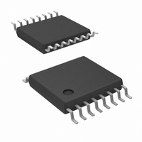
Physical Dimensions inches (millimeters) unless otherwise noted Order Number ADC108S052CIMT, ADC108S052CIMTX 16-Lead TSSOP NS Package Number MTC16 17 www.national.com ...
Page 18
... For more National Semiconductor product information and proven design tools, visit the following Web sites at: www.national.com Products Amplifiers www.national.com/amplifiers Audio www.national.com/audio Clock and Timing www.national.com/timing Data Converters www.national.com/adc Interface www.national.com/interface LVDS www.national.com/lvds Power Management www.national.com/power Switching Regulators www.national.com/switchers LDOs www.national.com/ldo LED Lighting www ...