ADC108S052CIMT/NOPB National Semiconductor, ADC108S052CIMT/NOPB Datasheet - Page 16
ADC108S052CIMT/NOPB
Manufacturer Part Number
ADC108S052CIMT/NOPB
Description
ADC 10BIT 8CH 200-500KSPS
Manufacturer
National Semiconductor
Series
PowerWise®r
Datasheet
1.ADC108S052CIMTNOPB.pdf
(18 pages)
Specifications of ADC108S052CIMT/NOPB
Number Of Bits
10
Sampling Rate (per Second)
500k
Data Interface
DSP, MICROWIRE™, QSPI™, Serial, SPI™
Number Of Converters
1
Power Dissipation (max)
7.5mW
Voltage Supply Source
Analog and Digital
Operating Temperature
-40°C ~ 105°C
Mounting Type
Surface Mount
Package / Case
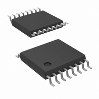
16-TSSOP (0.173", 4.40mm Width)
For Use With
ADC108S052EVAL - BOARD EVALUATION FOR ADC108S052
Lead Free Status / RoHS Status
Lead free / RoHS Compliant
Other names
*ADC108S052CIMT
*ADC108S052CIMT/NOPB
ADC108S052CIMT
*ADC108S052CIMT/NOPB
ADC108S052CIMT


www.national.com
The first solution to keeping digital noise out of the analog
supply is to decouple the analog and digital supplies from
each other or use separate supplies for them. To keep noise
out of the digital supply, keep the output load capacitance as
small as practical. If the load capacitance is greater than 50
pF, use a 100 Ω series resistor at the ADC output, located as
close to the ADC output pin as practical. This will limit the
charge and discharge current of the output capacitance and
improve noise performance. Since the series resistor and the
load capacitance form a low frequency pole, verify signal in-
tegrity once the series resistor has been added.
2.3 LAYOUT AND GROUNDING
Capacitive coupling between the noisy digital circuitry and the
sensitive analog circuitry can lead to poor performance. The
solution is to keep the analog circuitry separated from the
digital circuitry and the clock line as short as possible.
Digital circuits create substantial supply and ground current
transients. The logic noise generated could have significant
impact upon system noise performance. To avoid perfor-
mance degradation of the ADC108S052 due to supply noise,
do not use the same supply for the ADC108S052 that is used
for digital logic.
Generally, analog and digital lines should cross each other at
90° to avoid crosstalk. However, to maximize accuracy in high
16
resolution systems, avoid crossing analog and digital lines al-
together. It is important to keep clock lines as short as possi-
ble and isolated from ALL other lines, including other digital
lines. In addition, the clock line should also be treated as a
transmission line and be properly terminated.
The analog input should be isolated from noisy signal traces
to avoid coupling of spurious signals into the input. Any ex-
ternal component (e.g., a filter capacitor) connected between
the converter's input pins and ground or to the reference input
pin and ground should be connected to a very clean point in
the ground plane.
We recommend the use of a single, uniform ground plane and
the use of split power planes. The power planes should be
located within the same board layer. All analog circuitry (input
amplifiers, filters, reference components, etc.) should be
placed over the analog power plane. All digital circuitry and I/
O lines should be placed over the digital power plane. Fur-
thermore, all components in the reference circuitry and the
input signal chain that are connected to ground should be
connected together with short traces and enter the analog
ground plane at a single, quiet point.
Related parts for ADC108S052CIMT/NOPB
Image
Part Number
Description
Manufacturer
Datasheet
Request
R

Part Number:
Description:
National Semiconductor [8-Bit D/A Converter]
Manufacturer:
National Semiconductor
Datasheet:
Part Number:
Description:
National Semiconductor [Media Coprocessor]
Manufacturer:
National Semiconductor
Datasheet:
Part Number:
Description:
Digitally Controlled Tone and Volume Circuit with Stereo Audio Power Amplifier, Microphone Preamp Stage and National 3D Sound
Manufacturer:
National Semiconductor
Datasheet:
Part Number:
Description:
Digitally Controlled Tone and Volume Circuit with Stereo Audio Power Amplifier, Microphone Preamp Stage and National 3D Sound
Manufacturer:
National Semiconductor
Datasheet:
Part Number:
Description:
AC97 Rev 2 Codec with Sample Rate Conversion and National 3D Sound
Manufacturer:
National Semiconductor
Part Number:
Description:
Manufacturer:
National Semiconductor
Datasheet:
Part Number:
Description:
Manufacturer:
National Semiconductor
Datasheet:
Part Number:
Description:
General Purpose, Low Voltage, Low Power, Rail-to-Rail Output Operational Amplifiers
Manufacturer:
National Semiconductor
Datasheet:
Part Number:
Description:
8-bit 20 MSPS flash A/D converter.
Manufacturer:
National Semiconductor
Datasheet:
Part Number:
Description:
Low Noise Quad Operational Amplifier
Manufacturer:
National Semiconductor
Datasheet:
Part Number:
Description:
Quad Differential Line Receivers
Manufacturer:
National Semiconductor
Datasheet:
Part Number:
Description:
Quad High Speed Trapezoidal? Bus Transceiver
Manufacturer:
National Semiconductor
Datasheet:
Part Number:
Description:
Dual Line Receiver
Manufacturer:
National Semiconductor
Datasheet:
Part Number:
Description:
TTL to 10k ECL Level Translator with Latch
Manufacturer:
National Semiconductor
Datasheet: