ADC108S052CIMT/NOPB National Semiconductor, ADC108S052CIMT/NOPB Datasheet - Page 7
ADC108S052CIMT/NOPB
Manufacturer Part Number
ADC108S052CIMT/NOPB
Description
ADC 10BIT 8CH 200-500KSPS
Manufacturer
National Semiconductor
Series
PowerWise®r
Datasheet
1.ADC108S052CIMTNOPB.pdf
(18 pages)
Specifications of ADC108S052CIMT/NOPB
Number Of Bits
10
Sampling Rate (per Second)
500k
Data Interface
DSP, MICROWIRE™, QSPI™, Serial, SPI™
Number Of Converters
1
Power Dissipation (max)
7.5mW
Voltage Supply Source
Analog and Digital
Operating Temperature
-40°C ~ 105°C
Mounting Type
Surface Mount
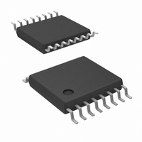
Package / Case
16-TSSOP (0.173", 4.40mm Width)
For Use With
ADC108S052EVAL - BOARD EVALUATION FOR ADC108S052
Lead Free Status / RoHS Status
Lead free / RoHS Compliant
Other names
*ADC108S052CIMT
*ADC108S052CIMT/NOPB
ADC108S052CIMT
*ADC108S052CIMT/NOPB
ADC108S052CIMT


Specification Definitions
ACQUISITION TIME is the time required for the ADC to ac-
quire the input voltage. During this time, the hold capacitor is
charged by the input voltage.
APERTURE DELAY is the time between the fourth falling
edge of SCLK and the time when the input signal is internally
acquired or held for conversion.
CONVERSION TIME is the time required, after the input volt-
age is acquired, for the ADC to convert the input voltage to a
digital word.
CHANNEL-TO-CHANNEL ISOLATION is resistance to cou-
pling of energy from one channel into another channel.
CROSSTALK is the coupling of energy from one channel into
another channel. This is similar to Channel-to-Channel Isola-
tion, except for the sign of the data.
DIFFERENTIAL NON-LINEARITY (DNL) is the measure of
the maximum deviation from the ideal step size of 1 LSB.
DUTY CYCLE is the ratio of the time that a repetitive digital
waveform is high to the total time of one period. The specifi-
cation here refers to the SCLK.
EFFECTIVE NUMBER OF BITS (ENOB, or EFFECTIVE
BITS) is another method of specifying Signal-to-Noise and
Distortion or SINAD. ENOB is defined as (SINAD - 1.76) / 6.02
and says that the converter is equivalent to a perfect ADC of
this (ENOB) number of bits.
FULL POWER BANDWIDTH is a measure of the frequency
at which the reconstructed output fundamental drops 3 dB
below its low frequency value for a full scale input.
FULL SCALE ERROR (FSE) is a measure of how far the last
code transition is from the ideal 1½ LSB below V
defined as:
where V
mum code occurs. FSE can be expressed in Volts, LSB or
percent of full scale range.
GAIN ERROR is the deviation of the last code transition
(111...110) to (111...111) from the ideal (V
adjusting for offset error.
INTEGRAL NON-LINEARITY (INL) is a measure of the de-
viation of each individual code from a line drawn from negative
full scale (½ LSB below the first code transition) through pos-
itive full scale (½ LSB above the last code transition). The
deviation of any given code from this straight line is measured
from the center of that code value.
max
is the voltage at which the transition to the maxi-
V
FSE
= V
max
+ 1.5 LSB – V
REF
REF
+
- 1.5 LSB), after
REF
+
and is
7
INTERMODULATION DISTORTION (IMD) is the creation of
additional spectral components as a result of two sinusoidal
frequencies being applied to an individual ADC input at the
same time. It is defined as the ratio of the power in both the
second or the third order intermodulation products to the pow-
er in one of the original frequencies. Second order products
are f
quencies. Third order products are (2f
IMD is usually expressed in dB.
MISSING CODES are those output codes that will never ap-
pear at the ADC outputs. The ADC108S052 is guaranteed not
to have any missing codes.
OFFSET ERROR is the deviation of the first code transition
(000...000) to (000...001) from the ideal (i.e. GND + 0.5 LSB).
SIGNAL TO NOISE RATIO (SNR) is the ratio, expressed in
dB, of the rms value of the input signal to the rms value of the
sum of all other spectral components below one-half the sam-
pling frequency, not including d.c. or the harmonics included
in THD.
SIGNAL TO NOISE PLUS DISTORTION (S/N+D or
SINAD) Is the ratio, expressed in dB, of the rms value of the
input signal to the rms value of all of the other spectral com-
ponents below half the clock frequency, including harmonics
but excluding d.c.
SPURIOUS FREE DYNAMIC RANGE (SFDR) is the differ-
ence, expressed in dB, between the rms values of the input
signal and the peak spurious signal where a spurious signal
is any signal present in the output spectrum that is not present
at the input, including harmonics but excluding d.c.
TOTAL HARMONIC DISTORTION (THD) is the ratio, ex-
pressed in dBc, of the rms total of the first five harmonic
components at the output to the rms level of the input signal
frequency as seen at the output. THD is calculated as
where A
put and A
harmonic frequencies.
THROUGHPUT TIME is the minimum time required between
the start of two successive conversions. It is the acquisition
time plus the conversion and read out times. In the case of
the ADC108S052, this is 16 SCLK periods.
a
± f
f1
b
, where f
is the RMS power of the input frequency at the out-
f2
through A
a
and f
f6
are the RMS power in the first 5
b
are the two sine wave input fre-
a
± f
b
) and (f
www.national.com
a
± 2f
b
).
Related parts for ADC108S052CIMT/NOPB
Image
Part Number
Description
Manufacturer
Datasheet
Request
R

Part Number:
Description:
National Semiconductor [8-Bit D/A Converter]
Manufacturer:
National Semiconductor
Datasheet:
Part Number:
Description:
National Semiconductor [Media Coprocessor]
Manufacturer:
National Semiconductor
Datasheet:
Part Number:
Description:
Digitally Controlled Tone and Volume Circuit with Stereo Audio Power Amplifier, Microphone Preamp Stage and National 3D Sound
Manufacturer:
National Semiconductor
Datasheet:
Part Number:
Description:
Digitally Controlled Tone and Volume Circuit with Stereo Audio Power Amplifier, Microphone Preamp Stage and National 3D Sound
Manufacturer:
National Semiconductor
Datasheet:
Part Number:
Description:
AC97 Rev 2 Codec with Sample Rate Conversion and National 3D Sound
Manufacturer:
National Semiconductor
Part Number:
Description:
Manufacturer:
National Semiconductor
Datasheet:
Part Number:
Description:
Manufacturer:
National Semiconductor
Datasheet:
Part Number:
Description:
General Purpose, Low Voltage, Low Power, Rail-to-Rail Output Operational Amplifiers
Manufacturer:
National Semiconductor
Datasheet:
Part Number:
Description:
8-bit 20 MSPS flash A/D converter.
Manufacturer:
National Semiconductor
Datasheet:
Part Number:
Description:
Low Noise Quad Operational Amplifier
Manufacturer:
National Semiconductor
Datasheet:
Part Number:
Description:
Quad Differential Line Receivers
Manufacturer:
National Semiconductor
Datasheet:
Part Number:
Description:
Quad High Speed Trapezoidal? Bus Transceiver
Manufacturer:
National Semiconductor
Datasheet:
Part Number:
Description:
Dual Line Receiver
Manufacturer:
National Semiconductor
Datasheet:
Part Number:
Description:
TTL to 10k ECL Level Translator with Latch
Manufacturer:
National Semiconductor
Datasheet: