ADC108S052CIMT/NOPB National Semiconductor, ADC108S052CIMT/NOPB Datasheet - Page 3
ADC108S052CIMT/NOPB
Manufacturer Part Number
ADC108S052CIMT/NOPB
Description
ADC 10BIT 8CH 200-500KSPS
Manufacturer
National Semiconductor
Series
PowerWise®r
Datasheet
1.ADC108S052CIMTNOPB.pdf
(18 pages)
Specifications of ADC108S052CIMT/NOPB
Number Of Bits
10
Sampling Rate (per Second)
500k
Data Interface
DSP, MICROWIRE™, QSPI™, Serial, SPI™
Number Of Converters
1
Power Dissipation (max)
7.5mW
Voltage Supply Source
Analog and Digital
Operating Temperature
-40°C ~ 105°C
Mounting Type
Surface Mount
Package / Case
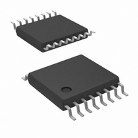
16-TSSOP (0.173", 4.40mm Width)
For Use With
ADC108S052EVAL - BOARD EVALUATION FOR ADC108S052
Lead Free Status / RoHS Status
Lead free / RoHS Compliant
Other names
*ADC108S052CIMT
*ADC108S052CIMT/NOPB
ADC108S052CIMT
*ADC108S052CIMT/NOPB
ADC108S052CIMT


STATIC CONVERTER CHARACTERISTICS
INL
DNL
V
OEM
FSE
FSEM
DYNAMIC CONVERTER CHARACTERISTICS
FPBW
SINAD
SNR
THD
SFDR
ENOB
ISO
IMD
ANALOG INPUT CHARACTERISTICS
V
I
C
DCL
OFF
IN
Symbol
INA
Absolute Maximum Ratings
If Military/Aerospace specified devices are required,
please contact the National Semiconductor Sales Office/
Distributors for availability and specifications.
ADC108S052 Converter Electrical Characteristics
The following specifications apply for V
ksps to 500 ksps, and C
C.
Analog Supply Voltage V
Digital Supply Voltage V
Voltage on Any Pin to GND
Input Current at Any Pin
Package Input
Power Dissipation at T
ESD Susceptibility
For soldering specifications:
Junction Temperature
Storage Temperature
Machine Model
see product folder at www.national.com and
www.national.com/ms/MS/MS-SOLDERING.pdf
Human Body Model
Resolution with No Missing Codes
Integral Non-Linearity (End Point
Method)
Differential Non-Linearity
Offset Error
Offset Error Match
Full Scale Error
Full Scale Error Match
Full Power Bandwidth (−3dB)
Signal-to-Noise Plus Distortion Ratio
Signal-to-Noise Ratio
Total Harmonic Distortion
Spurious-Free Dynamic Range
Effective Number of Bits
Channel-to-Channel Isolation
Intermodulation Distortion, Second
Order Terms
Intermodulation Distortion, Third Order
Terms
Input Range
DC Leakage Current
Input Capacitance
Current(Note
(Note
A
L
Parameter
D
= 25°C
(Note
A
5)
= 50pF, unless otherwise noted. Boldface limits apply for T
3)
3)
A
−0.3V to V
= V
−0.3V to V
−65°C to +150°C
D
= +2.7V to +5.25V, AGND = DGND = 0V, f
−0.3V to 6.5V
See
(Note
max 6.5V
f
f
f
f
f
f
f
f
Track Mode
Hold Mode
A
IN
IN
IN
IN
IN
IN
a
a
(Note
±10 mA
±20 mA
A
+150°C
+ 0.3V,
= 19.5 kHz, f
= 19.5 kHz, f
2500V
= 40.2 kHz, −0.02 dBFS
= 40.2 kHz, −0.02 dBFS
= 40.2 kHz, −0.02 dBFS
= 40.2 kHz, −0.02 dBFS
= 40.2 kHz
= 20 kHz
1)
+0.3V
250V
4)
3
Conditions
b
b
= 20.5 kHz
= 20.5 kHz
Operating Ratings
Package Thermal Resistance
Operating Temperature
V
V
Digital Input Voltage
Analog Input Voltage
Clock Frequency
A
D
Supply Voltage
Supply Voltage
16-lead TSSOP on 4-
layer, 2 oz. PCB
Package
(Note
A
SCLK
= T
7)
MIN
Typical
0 to V
±0.06
±0.06
−87.4
−85.1
−81.6
= 3.2 MHz to 8 MHz, f
±0.1
±0.2
+0.3
+0.1
61.8
61.8
83.2
9.98
78.6
33
to T
8
3
A
MAX
(Note
: all other limits T
(Note
Limits
−74.5
±0.4
±0.4
±0.7
±0.4
±0.4
±0.4
61.3
61.4
76.0
9.89
96°C / W
±1
10
1,
−40°C
θ
Note
50 kHz to 16 MHz
6)
JA
+2.7V to +5.25V
≤
2)
SAMPLE
+2.7V to V
www.national.com
T
LSB (max)
LSB (max)
LSB (max)
LSB (max)
LSB (max)
LSB (min)
Bits (min)
A
dB (max)
µA (max)
dB (min)
dB (min)
dB (min)
0V to V
0V to V
≤
Units
A
MHz
Bits
dB
dB
dB
pF
pF
+105°
V
= 25°
= 200
C
A
A
A
Related parts for ADC108S052CIMT/NOPB
Image
Part Number
Description
Manufacturer
Datasheet
Request
R

Part Number:
Description:
National Semiconductor [8-Bit D/A Converter]
Manufacturer:
National Semiconductor
Datasheet:
Part Number:
Description:
National Semiconductor [Media Coprocessor]
Manufacturer:
National Semiconductor
Datasheet:
Part Number:
Description:
Digitally Controlled Tone and Volume Circuit with Stereo Audio Power Amplifier, Microphone Preamp Stage and National 3D Sound
Manufacturer:
National Semiconductor
Datasheet:
Part Number:
Description:
Digitally Controlled Tone and Volume Circuit with Stereo Audio Power Amplifier, Microphone Preamp Stage and National 3D Sound
Manufacturer:
National Semiconductor
Datasheet:
Part Number:
Description:
AC97 Rev 2 Codec with Sample Rate Conversion and National 3D Sound
Manufacturer:
National Semiconductor
Part Number:
Description:
Manufacturer:
National Semiconductor
Datasheet:
Part Number:
Description:
Manufacturer:
National Semiconductor
Datasheet:
Part Number:
Description:
General Purpose, Low Voltage, Low Power, Rail-to-Rail Output Operational Amplifiers
Manufacturer:
National Semiconductor
Datasheet:
Part Number:
Description:
8-bit 20 MSPS flash A/D converter.
Manufacturer:
National Semiconductor
Datasheet:
Part Number:
Description:
Low Noise Quad Operational Amplifier
Manufacturer:
National Semiconductor
Datasheet:
Part Number:
Description:
Quad Differential Line Receivers
Manufacturer:
National Semiconductor
Datasheet:
Part Number:
Description:
Quad High Speed Trapezoidal? Bus Transceiver
Manufacturer:
National Semiconductor
Datasheet:
Part Number:
Description:
Dual Line Receiver
Manufacturer:
National Semiconductor
Datasheet:
Part Number:
Description:
TTL to 10k ECL Level Translator with Latch
Manufacturer:
National Semiconductor
Datasheet: