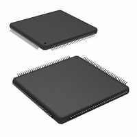
ADC08D500CIYB/NOPB National Semiconductor, ADC08D500CIYB/NOPB Datasheet - Page 11

ADC08D500CIYB/NOPB
Manufacturer Part Number
ADC08D500CIYB/NOPB
Description
IC ADC 8BIT 500MSPS DUAL 128LQFP
Manufacturer
National Semiconductor
Series
PowerWise®r
Specifications of ADC08D500CIYB/NOPB
Number Of Bits
8
Sampling Rate (per Second)
500M
Data Interface
Serial
Number Of Converters
2
Power Dissipation (max)
1.78W
Voltage Supply Source
Single Supply
Operating Temperature
-40°C ~ 85°C
Mounting Type
Surface Mount
Package / Case
128-LQFP Exposed Pad
Lead Free Status / RoHS Status
Lead free / RoHS Compliant
Other names
*ADC08D500CIYB
*ADC08D500CIYB/NOPB
ADC08D500CIYB
*ADC08D500CIYB/NOPB
ADC08D500CIYB
Available stocks
Company
Part Number
Manufacturer
Quantity
Price
Company:
Part Number:
ADC08D500CIYB/NOPB
Manufacturer:
Texas Instruments
Quantity:
10 000
www.national.com
R
ANALOG OUTPUT CHARACTERISTICS
V
V
TC V
C
V
V
TC V
C
TEMPERATURE DIODE CHARACTERISTICS
ΔV
CHANNEL-TO-CHANNEL CHARACTERISTICS
X-TALK
X-TALK
CLOCK INPUT CHARACTERISTICS
V
I
C
DIGITAL CONTROL PIN CHARACTERISTICS
V
V
C
DIGITAL OUTPUT CHARACTERISTICS
V
Δ V
I
Symbol
CMO
CMO_LVL
CMO
BG
ID
IH
IL
OD
IN
LOAD
LOAD
IN
IN
BE
O DIFF
CMO
BG
V
BG
Differential Input Resistance
Common Mode Output Voltage
V
Coupling mode
Common Mode Output Voltage
Temperature Coefficient
Maximum V
Bandgap Reference Output Voltage
Bandgap Reference Voltage
Temperature Coefficient
Maximum Bandgap Reference Load
Capacitance
Temperature Diode Voltage
Offset Error Match
Positive Full-Scale Error Match
Negative Full-Scale Error Match
Phase Matching (I, Q)
Crosstalk from I (Aggressor) to Q
(Victim) Channel
Crosstalk from Q (Aggressor) to I
(Victim) Channel
Differential Clock Input Level
Input Current
Input Capacitance
Logic High Input Voltage
Logic Low Input Voltage
Input Capacitance
LVDS Differential Output Voltage
Change in LVDS Output Swing
Between Logic Levels
CMO
input threshold to set DC
CMO
Parameter
load Capacitance
(Note
(Note
10,
11,
Note
Note
11)
13) Each input to ground
V
V
T
I
T
192 µA vs. 12 µA,
T
192 µA vs. 12 µA,
T
Zero offset selected in Control Register
Zero offset selected in Control Register
F
Aggressor = 867 MHz F.S.
Victim = 100 MHz F.S.
Aggressor = 867 MHz F.S.
Victim = 100 MHz F.S.
Sine Wave Clock
Square Wave Clock
V
Differential
Each input to ground
(Note
(Note
Measured differentially, OutV = V
V
Measured differentially, OutV = GND,
V
BG
A
A
J
J
IN
A
A
IN
BG
BG
= 25°C
= 85°C
= −40°C to +85°C
= −40°C to +85°C, I
= 1.8V
= 2.0V
= ±100 µA
= 1.0 GHz
= 0 or V
= Floating,
= Floating,
12)
12)
IN
Conditions
10
= V
(Note
(Note
A
15)
15)
BG
= ±100 µA
A
,
(Note
Typical
71.23
85.54
1.26
0.60
0.66
1.26
0.02
100
118
−71
710
510
< 1
-71
0.6
0.6
1.5
1.2
28
±1
±1
1
1
1
8)
0.85 x V
0.15 x V
(Note
Limits
0.95
1.45
1.20
1.33
106
400
920
280
720
0.4
2.0
0.4
2.0
94
80
80
8)
A
A
mV
mV
mV
mV
V
V
V
V
(Limits)
Ω (max)
V (max)
V (max)
V (max)
Ω (min)
ppm/°C
ppm/°C
Degree
P-P
P-P
V (min)
V (min)
V (min)
P-P
P-P
Units
P-P
P-P
P-P
P-P
LSB
LSB
LSB
mV
mV
mV
dB
dB
µA
pF
pF
pF
pF
pF
V
V
(max)
(max)
(min)
(min)
(max)
(max)
(min)
(min)


