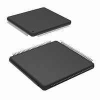
ADC08D500CIYB/NOPB National Semiconductor, ADC08D500CIYB/NOPB Datasheet - Page 12

ADC08D500CIYB/NOPB
Manufacturer Part Number
ADC08D500CIYB/NOPB
Description
IC ADC 8BIT 500MSPS DUAL 128LQFP
Manufacturer
National Semiconductor
Series
PowerWise®r
Specifications of ADC08D500CIYB/NOPB
Number Of Bits
8
Sampling Rate (per Second)
500M
Data Interface
Serial
Number Of Converters
2
Power Dissipation (max)
1.78W
Voltage Supply Source
Single Supply
Operating Temperature
-40°C ~ 85°C
Mounting Type
Surface Mount
Package / Case
128-LQFP Exposed Pad
Lead Free Status / RoHS Status
Lead free / RoHS Compliant
Other names
*ADC08D500CIYB
*ADC08D500CIYB/NOPB
ADC08D500CIYB
*ADC08D500CIYB/NOPB
ADC08D500CIYB
Available stocks
Company
Part Number
Manufacturer
Quantity
Price
Company:
Part Number:
ADC08D500CIYB/NOPB
Manufacturer:
Texas Instruments
Quantity:
10 000
V
V
Δ V
I
Z
V
V
POWER SUPPLY CHARACTERISTICS
I
I
P
PSRR1
PSRR2
AC ELECTRICAL CHARACTERISTICS
f
f
f
t
t
t
t
t
t
t
t
t
t
t
t
t
OS
A
DR
CLK1
CLK2
CLK2
CL
CH
RS
RH
SD
RPW
LHT
HLT
OSK
SU
H
AD
AJ
O
Symbol
OS
OS
OH
OL
D
OS
Output Offset Voltage, see
Output Offset Voltage, see
Output Offset Voltage Change
Between Logic Levels
Output Short Circuit Current
Differential Output Impedance
Cal_Run High level output
Cal_Run Low level output
Analog Supply Current
Output Driver Supply Current
Power Consumption
D.C. Power Supply Rejection Ratio
A.C. Power Supply Rejection Ratio
Maximum Input Clock Frequency
Minimum Input Clock Frequency
Minimum Input Clock Frequency
Input Clock Duty Cycle
Input Clock Duty Cycle
Input Clock Low Time
Input Clock High Time
DCLK Duty Cycle
Reset Setup Time
Reset Hold Time
Synchronizing Edge to DCLK Output
Delay
Reset Pulse Width
Differential Low to High Transition
Time
Differential High to Low Transition
Time
DCLK to Data Output Skew
Data to DCLK Set-Up Time
DCLK to Data Hold Time
Sampling (Aperture) Delay
Aperture Jitter
Parameter
Figure 1
Figure 1
V
V
Output+ & Output- connected to 0.8V
I
I
PD = PDQ = Low
PD = Low, PDQ = High
PD = PDQ = High
PD = PDQ = Low
PD = Low, PDQ = High
PD = PDQ = High
PD = PDQ = Low
PD = Low, PDQ = High
PD = PDQ = High
Change in Full Scale Error with change
in V
248 MHz, 50mV
Normal Mode (non DES) or DES Mode
Normal Mode (non DES)
DES Mode
200 MHz
500 MHz (Normal
450 MHz
500 MHz (DES
(Note
(Note
(Note
(Note
(Note
f
f
(Note
10% to 90%, C
10% to 90%, C
50% of DCLK transition to 50% of Data
transition, SDR Mode
and DDR Mode, 0° DCLK
DDR Mode, 90° DCLK
DDR Mode, 90° DCLK
Input CLK+ Fall to Acquisition of Data
OH
OH
CLKIN
CLKIN
BG
BG
= -400uA
= 400uA
A
= Floating
= V
from 1.8V to 2.0V
= 500 MHz
= 200 MHz
12)
12)
12)
12)
12)
11)
A
(Note
≤
≤
Input clock frequency
Input clock frequency
(Note
Conditions
(Note
11
L
L
Mode)(Note
15)
P-P
= 2.5 pF
= 2.5 pF
Mode)(Note
12)
riding on V
12)
(Note
(Note
(Note
12)
12)
12)
A
12)
12)
≤
≤
(Note
Typical
0.012
1200
1.65
0.15
3.53
3.85
800
100
561
340
200
112
200
450
500
500
150
250
250
250
±50
1.8
1.4
0.8
3.5
1.3
0.4
±1
−4
30
51
50
50
50
2
2
8)
(Note
Limits
1.78
665
408
275
157
500
400
400
1.5
0.3
1.0
20
80
20
80
45
55
4
8)
Clock Cycles
www.national.com
MHz (min)
mA (max)
mA (max)
mA (max)
ps (max)
W (max)
% (max)
% (max)
% (max)
(Limits)
ps (min)
ps (min)
% (min)
% (min)
% (min)
ps rms
Ohms
Units
(min)
MHz
MHz
mW
mV
mV
mV
mA
mA
mA
mA
dB
dB
ps
ps
ns
ps
ps
ns
ns
ns
W
V
V


