ADC08D500CIYB/NOPB National Semiconductor, ADC08D500CIYB/NOPB Datasheet - Page 32
ADC08D500CIYB/NOPB
Manufacturer Part Number
ADC08D500CIYB/NOPB
Description
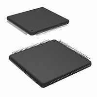
IC ADC 8BIT 500MSPS DUAL 128LQFP
Manufacturer
National Semiconductor
Series
PowerWise®r
Specifications of ADC08D500CIYB/NOPB
Number Of Bits
8
Sampling Rate (per Second)
500M
Data Interface
Serial
Number Of Converters
2
Power Dissipation (max)
1.78W
Voltage Supply Source
Single Supply
Operating Temperature
-40°C ~ 85°C
Mounting Type
Surface Mount
Package / Case
128-LQFP Exposed Pad
Lead Free Status / RoHS Status
Lead free / RoHS Compliant
Other names
*ADC08D500CIYB
*ADC08D500CIYB/NOPB
ADC08D500CIYB
*ADC08D500CIYB/NOPB
ADC08D500CIYB
Available stocks
Company
Part Number
Manufacturer
Quantity
Price
Company:

Part Number:
ADC08D500CIYB/NOPB
Manufacturer:
Texas Instruments
Quantity:
10 000


at the balun output. Or, 25 Ohms to virtual ground at each of
the balun output terminals.
Looking into the balun, the source sees the impedance of the
first coil in series with the impedance at the output of that coil.
Since the transformer has a 1:1 turns ratio, the impedance
across the first coil is exactly the same as that at the output
of the second coil, namely 25 Ohms to virtual ground. So, the
25 Ohms across the first coil in series with the 25 Ohms at its
output gives 50 Ohms total impedance to match the source.
2.2.2 Out Of Range (OR) Indication
When the conversion result is clipped the Out of Range output
is activated such that OR+ goes high and OR- goes low. This
output is active as long as accurate data on either or both of
the buses would be outside the range of 00h to FFh.
2.2.3 Full-Scale Input Range
As with all A/D Converters, the input range is determined by
the value of the ADC's reference voltage. The reference volt-
age of the ADC08D500 is derived from an internal band-gap
reference. The FSR pin controls the effective reference volt-
age of the ADC08D500 such that the differential full-scale
input range at the analog inputs is 870 mV
pin high, or is 650 mV
tained with FSR high, but better distortion and SFDR are
obtained with the FSR pin low.
2.3 THE CLOCK INPUTS
The ADC08D500 has differential LVDS clock inputs, CLK+
and CLK-, which must be driven with a differential, a.c. cou-
pled clock signal as indicated in
ADC08D500 is tested and its performance is guaranteed with
a differential 500 MHz clock, it typically will function well with
clock frequencies indicated in the Electrical Characteristics
Table. The clock inputs are internally terminated and biased.
Operation up to the sample rates indicated in the Electrical
Characteristics Table is typically possible if the maximum am-
bient temperatures indicated are not exceeded. Operating at
higher sample rates than indicated for the given ambient tem-
perature may result in reduced device reliability and product
lifetime. This is because of the higher power consumption and
die temperatures at high sample rates. Important also for re-
liability is proper thermal management . See Section 2.6.2.
The differential Clock line pair should have a characteristic
impedance of 100Ω and be terminated at the clock source in
that (100Ω) characteristic impedance. The clock line should
be as short and as direct as possible. The ADC08D500 clock
input is internally terminated with an untrimmed 100Ω resis-
tor.
Insufficient clock levels will result in poor dynamic perfor-
mance. Excessively high clock levels could cause a change
FIGURE 14. Differential (LVDS) Clock Connection
P-P
with FSR pin low. Best SNR is ob-
Figure
20121447
14. Although the
P-P
with the FSR
31
in the analog input offset voltage. To avoid these problems,
keep the clock level within the range specified in the Electrical
Characteristics Table.
The low and high times of the input clock signal can affect the
performance of any A/D Converter. The ADC08D1000 fea-
tures a duty cycle clock correction circuit which can maintain
performance over temperature even in DES mode. The ADC
will meet its performance specification if the input clock high
and low times are maintained within the range (20/80% ratio)
as specified in the Electrical Characteristics Table.
High speed, high performance ADCs such as the
ADC08D500 require a very stable clock signal with minimum
phase noise or jitter. ADC jitter requirements are defined by
the ADC resolution (number of bits), maximum ADC input fre-
quency and the input signal amplitude relative to the ADC
input full scale range. The maximum jitter (the sum of the jitter
from all sources) allowed to prevent a jitter-induced reduction
in SNR is found to be
where t
V
full-scale range of the ADC, "N" is the ADC resolution in bits
and f
analog input.
Note that the maximum jitter described above is the arithmetic
sum of the jitter from all sources, including that in the ADC
clock, that added by the system to the ADC clock and input
signals and that added by the ADC itself. Since the effective
jitter added by the ADC is beyond user control, the best the
user can do is to keep the sum of the externally added clock
jitter and the jitter added by the analog circuitry to the analog
signal to a minimum.
Clock amplitudes above those specified in the Electrical Char-
acteristics Table may result in increased input offset voltage.
This would cause the converter to produce an output code
other than the expected 127/128 when both input pins are at
the same potential.
2.4 CONTROL PINS
Six control pins (without the use of the serial interface) provide
a wide range of possibilities in the operation of the
ADC08D500 and facilitate its use. These control pins provide
Full-Scale Input Range setting, Self Calibration, Calibration
Delay, Output Edge Synchronization choice, LVDS Output
Level choice and a Power Down feature.
2.4.1 Full-Scale Input Range Setting
The input full-scale range can be selected to be either 650
mV
(pin 14) in the Normal Mode of operation. In the Extended
Control Mode, the input full-scale range may be set to be
anywhere from 560 mV
more information.
2.4.2 Self Calibration
The ADC08D500 self-calibration must be run to achieve
specified performance. The calibration procedure is run upon
power-up and can be run any time on command. The cali-
bration procedure is exactly the same whether there is a clock
present upon power up or if the clock begins some time after
application of power. The CalRun output indicator is high
while a calibration is in progress. Note that DCLK outputs are
not active during a calibration cycle, therefore it is not recom-
mended as a system clock.
IN(P-P)
P-P
IN
t
or 870 mV
J(MAX)
is the maximum input frequency, in Hertz, to the ADC
J(MAX)
is the peak-to-peak analog input signal, V
= (V
is the rms total of all jitter sources in seconds,
IN(P-P)
P-P
, as selected with the FSR control input
P-P
/ V
INFSR
to 840 mV
) x (1/(2
P-P
(N+1)
. See Section 2.2 for
x
π
x f
www.national.com
INFSR
IN
))
is the
Related parts for ADC08D500CIYB/NOPB
Image
Part Number
Description
Manufacturer
Datasheet
Request
R

Part Number:
Description:
National Semiconductor [8-Bit D/A Converter]
Manufacturer:
National Semiconductor
Datasheet:
Part Number:
Description:
National Semiconductor [Media Coprocessor]
Manufacturer:
National Semiconductor
Datasheet:
Part Number:
Description:
Digitally Controlled Tone and Volume Circuit with Stereo Audio Power Amplifier, Microphone Preamp Stage and National 3D Sound
Manufacturer:
National Semiconductor
Datasheet:
Part Number:
Description:
Digitally Controlled Tone and Volume Circuit with Stereo Audio Power Amplifier, Microphone Preamp Stage and National 3D Sound
Manufacturer:
National Semiconductor
Datasheet:
Part Number:
Description:
AC97 Rev 2 Codec with Sample Rate Conversion and National 3D Sound
Manufacturer:
National Semiconductor
Part Number:
Description:
Manufacturer:
National Semiconductor
Datasheet:
Part Number:
Description:
Manufacturer:
National Semiconductor
Datasheet:
Part Number:
Description:
General Purpose, Low Voltage, Low Power, Rail-to-Rail Output Operational Amplifiers
Manufacturer:
National Semiconductor
Datasheet:
Part Number:
Description:
8-bit 20 MSPS flash A/D converter.
Manufacturer:
National Semiconductor
Datasheet:
Part Number:
Description:
Low Noise Quad Operational Amplifier
Manufacturer:
National Semiconductor
Datasheet:
Part Number:
Description:
Quad Differential Line Receivers
Manufacturer:
National Semiconductor
Datasheet:
Part Number:
Description:
Quad High Speed Trapezoidal? Bus Transceiver
Manufacturer:
National Semiconductor
Datasheet:
Part Number:
Description:
Dual Line Receiver
Manufacturer:
National Semiconductor
Datasheet:
Part Number:
Description:
TTL to 10k ECL Level Translator with Latch
Manufacturer:
National Semiconductor
Datasheet: