ADC083000CIYB/NOPB National Semiconductor, ADC083000CIYB/NOPB Datasheet - Page 12
ADC083000CIYB/NOPB
Manufacturer Part Number
ADC083000CIYB/NOPB
Description
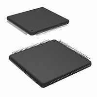
IC ADC 8BIT 3GSPS LP 128-LQFP
Manufacturer
National Semiconductor
Series
PowerWise®r
Datasheet
1.ADC083000CIYBNOPB.pdf
(40 pages)
Specifications of ADC083000CIYB/NOPB
Number Of Bits
8
Sampling Rate (per Second)
3G
Data Interface
Serial
Number Of Converters
2
Power Dissipation (max)
2.3W
Voltage Supply Source
Single Supply
Operating Temperature
-40°C ~ 85°C
Mounting Type
Surface Mount
Package / Case
128-LQFP Exposed Pad
Lead Free Status / RoHS Status
Lead free / RoHS Compliant
Other names
*ADC083000CIYB
*ADC083000CIYB/NOPB
ADC083000CIYB
*ADC083000CIYB/NOPB
ADC083000CIYB
Available stocks
Company
Part Number
Manufacturer
Quantity
Price
Company:

Part Number:
ADC083000CIYB/NOPB
Manufacturer:
IPS
Quantity:
2 300
Part Number:
ADC083000CIYB/NOPB
Manufacturer:
TI/德州仪器
Quantity:
20 000


www.national.com
AC ELECTRICAL CHARACTERISTICS - Sampling Clock
f
f
t
t
t
t
t
t
AC ELECTRICAL CHARACTERISTICS - Output Clock and Data (Note 16)
t
t
t
t
t
AC ELECTRICAL CHARACTERISTICS - Serial Interface Clock
f
t
t
AC ELECTRICAL CHARACTERISTICS - General Signals
t
t
t
t
t
t
t
t
CLK1
CLK2
CYC
LC
HC
AD
AJ
OD
LHT
HLT
SKEWO
OSU
OH
SCLK
SS
HS
SR
HR
PWR
WU
CAL
CAL_L
CAL_H
CalDly
Symbol
Maximum Input Clock Frequency Sampling rate is 2x clock input
Minimum Input Clock Frequency Sampling rate is 2x clock input
Input Clock Duty Cycle
Input Clock Low Time
Input Clock High Time
DCLK Duty Cycle
Sampling (Aperture) Delay
Aperture Jitter
Input Clock to Data Output Delay
(in addition to Pipeline Delay)
Pipeline Delay (Latency)
(Notes 11, 14)
LH Transition Time - Differential
HL Transition Time - Differential
DCLK to Data Output Skew
Data to DCLK Set-Up Time
DCLK to Data Hold Time
Serial Clock Frequency
Data to Serial Clock Setup Time (Note 11)
Data to Serial Clock Hold Time
Serial Clock Low Time
Serial Clock High Time
Setup Time DCLK_RST±
Hold Time DCLK_RST±
Pulse Width DCLK_RST±
PD low to Rated Accuracy
Conversion (Wake-Up Time)
Calibration Cycle Time
CAL Pin Low Time
CAL Pin High Time
Calibration delay
CalDly = Low
Calibration delay
CalDly = High
Parameter
500MHz
GHz (Note 12)
(Note 11)
(Note 11)
(Note 11)
Input CLK transition to Acquisition of
Data
50% of Input Clock transition to 50% of
Data transition
Dd Outputs
Db Outputs
Dc Outputs
Da Outputs
10% to 90%
10% to 90%
50% of DCLK transition to 50% of Data
transition, SDR Mode
and DDR Mode, 0° DCLK (Note 11)
DDR Mode, 90° DCLK (Note 12)
DDR Mode, 90° DCLK (Note 12)
(Note 11)
(Note 11)
(Note 12)
(Note 11)
(Note 11)
See Figure 8 (Note 11)
See Figure 8 (Note 11)
See Section 1.1.1, Figure 8, (Note 11)
See Section 1.1.1, Figure 8, (Note 11)
≤
Input clock frequency
Conditions
12
≤
1.5
1.4 x 10
(Note 8)
Typical
0.55
±50
500
333
333
150
150
570
555
1.4
3.7
2.5
50
50
67
90
30
1
1
5
(Note 8)
Limits
13.5
14.5
133
133
1.5
2
2
20
80
45
55
13
14
80
80
6
6
4
25
31
CLK± Cyc. (min)
CLK± Cyc. (min)
CLK± Cyc. (min)
CLK± Cyc. (min)
Input Clock
CLK± Cyc.
CLK± Cyc.
GHz (min)
ps (max)
% (max)
% (max)
(Limits)
ps (min)
ps (min)
ns (min)
ns (min)
ns (min)
ns (min)
% (min)
% (min)
ps rms
Cycles
(max)
Units
MHz
MHz
ns
ns
ps
ps
ps
ps
ps
ps
µs
Related parts for ADC083000CIYB/NOPB
Image
Part Number
Description
Manufacturer
Datasheet
Request
R

Part Number:
Description:
National Semiconductor [8-Bit D/A Converter]
Manufacturer:
National Semiconductor
Datasheet:
Part Number:
Description:
National Semiconductor [Media Coprocessor]
Manufacturer:
National Semiconductor
Datasheet:
Part Number:
Description:
Digitally Controlled Tone and Volume Circuit with Stereo Audio Power Amplifier, Microphone Preamp Stage and National 3D Sound
Manufacturer:
National Semiconductor
Datasheet:
Part Number:
Description:
Digitally Controlled Tone and Volume Circuit with Stereo Audio Power Amplifier, Microphone Preamp Stage and National 3D Sound
Manufacturer:
National Semiconductor
Datasheet:
Part Number:
Description:
AC97 Rev 2 Codec with Sample Rate Conversion and National 3D Sound
Manufacturer:
National Semiconductor
Part Number:
Description:
Manufacturer:
National Semiconductor
Datasheet:
Part Number:
Description:
Manufacturer:
National Semiconductor
Datasheet:
Part Number:
Description:
General Purpose, Low Voltage, Low Power, Rail-to-Rail Output Operational Amplifiers
Manufacturer:
National Semiconductor
Datasheet:
Part Number:
Description:
8-bit 20 MSPS flash A/D converter.
Manufacturer:
National Semiconductor
Datasheet:
Part Number:
Description:
Low Noise Quad Operational Amplifier
Manufacturer:
National Semiconductor
Datasheet:
Part Number:
Description:
Quad Differential Line Receivers
Manufacturer:
National Semiconductor
Datasheet:
Part Number:
Description:
Quad High Speed Trapezoidal? Bus Transceiver
Manufacturer:
National Semiconductor
Datasheet:
Part Number:
Description:
Dual Line Receiver
Manufacturer:
National Semiconductor
Datasheet:
Part Number:
Description:
TTL to 10k ECL Level Translator with Latch
Manufacturer:
National Semiconductor
Datasheet: