ADC083000CIYB/NOPB National Semiconductor, ADC083000CIYB/NOPB Datasheet - Page 31
ADC083000CIYB/NOPB
Manufacturer Part Number
ADC083000CIYB/NOPB
Description
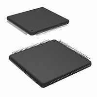
IC ADC 8BIT 3GSPS LP 128-LQFP
Manufacturer
National Semiconductor
Series
PowerWise®r
Datasheet
1.ADC083000CIYBNOPB.pdf
(40 pages)
Specifications of ADC083000CIYB/NOPB
Number Of Bits
8
Sampling Rate (per Second)
3G
Data Interface
Serial
Number Of Converters
2
Power Dissipation (max)
2.3W
Voltage Supply Source
Single Supply
Operating Temperature
-40°C ~ 85°C
Mounting Type
Surface Mount
Package / Case
128-LQFP Exposed Pad
Lead Free Status / RoHS Status
Lead free / RoHS Compliant
Other names
*ADC083000CIYB
*ADC083000CIYB/NOPB
ADC083000CIYB
*ADC083000CIYB/NOPB
ADC083000CIYB
Available stocks
Company
Part Number
Manufacturer
Quantity
Price
Company:

Part Number:
ADC083000CIYB/NOPB
Manufacturer:
IPS
Quantity:
2 300
Part Number:
ADC083000CIYB/NOPB
Manufacturer:
TI/德州仪器
Quantity:
20 000


2.0 Applications Information
2.1 THE REFERENCE VOLTAGE
The voltage reference for the ADC083000 is derived from a
1.254V bandgap reference, a buffered version of which is
made available at pin 31, V
output has an output current capability of ±100 μA. This ref-
erence voltage should be buffered if more current is required.
The internal bandgap-derived reference voltage has a nomi-
nal value of 600 mV or 820 mV, as determined by the FSR
pin and described in Section 1.1.4.
There is no provision for the use of an external reference volt-
age, but the full-scale input voltage can be adjusted through
a Configuration Register in the Extended Control mode, as
explained in Section 1.2.
Differential input signals up to the chosen full-scale level will
be digitized to 8 bits. Signal excursions beyond the full-scale
range will be clipped at the output. These large signal excur-
sions will also activate the OR output for the time that the
signal is out of range. See Section 2.2.2.
One extra feature of the V
the common mode voltage level of the LVDS outputs. The
output offset voltage (V
pin is used as an output or left unconnected. To raise the
LVDS offset voltage to a typical value of 1150mV the V
can be connected directly to the supply rails.
2.2 THE ANALOG INPUT
The analog input is a differential one to which the signal
source may be a.c. coupled or d.c. coupled. The full-scale
input range is selected with the FSR pin to be 600 mV
820 mV
560 mV
through the Serial Interface. For best performance, it is rec-
ommended
between 595 mV
mode because the internal DAC which sets the full-scale
range is not as linear at the ends of its range.
Table 6 gives the input to output relationship with the FSR pin
high when the normal (non-extended) mode is used. With the
FSR pin grounded, the millivolt values in Table 6 are reduced
to 75% of the values indicated. In the Enhanced Control
Mode, these values will be determined by the full scale range
and offset settings in the Control Registers.
RELATIONSHIP (Non-Extended Control Mode, FSR High)
The buffered analog inputs simplify the task of driving these
inputs and the RC pole that is generally used at sampling ADC
inputs is not required. If it is desired to use an amplifier circuit
before the ADC, use care in choosing an amplifier with ade-
quate noise and distortion performance and adequate gain at
the frequencies used for the application.
The Input impedance of V
(V
across the inputs and a capacitance from each of these inputs
V
V
CMO
V
V
CM
CM
CM
CM
TABLE 6. DIFFERENTIAL INPUT TO OUTPUT
− 102.5 mV
+ 102.5 mV
pin not grounded) consists of a precision 100Ω resistor
V
− 205mV
+ 205mV
V
P-P
P-P
IN
CM
+
, or can be adjusted to values between
and 840 mV
that
P-P
and 805 mV
V
V
the
V
V
CM
CM
OS
CM
CM
P-P
BG
+ 102.5 mV
) is typically 800mV when the V
−102.5 mV
IN+
V
+ 205mV
− 205mV
V
pin is that it can be used to raise
full-scale
IN
in the Extended Control mode
CM
BG
/ V
−
, for user convenience. This
IN-
P-P
in the d.c. coupled mode
in the Extended Control
range
Output Code
0111 1111 /
0000 0000
0100 0000
1000 0000
1100 0000
1111 1111
be
BG
P-P
kept
pin
BG
or
31
to ground. In the a.c. coupled mode, the input appears the
same except there is also a resistor of 50KΩ between each
analog input pin and the on-chip V
When the inputs are a.c. coupled, the V
grounded, as shown in Figure 11. This causes the on-chip
V
50KΩ resistors.
When the d.c. coupled mode is used, a precise common
mode voltage must be provided at the differential inputs. This
common mode voltage should track the V
that the V
The common mode output of the driving device should track
this change.
Full-scale distortion performance falls off rapidly as the input
common mode voltage deviates from V
result of using a very low supply voltage to minimize power.
Keep the input common voltage within 50 mV of V
Performance is as good in the d.c. coupled mode as it is in
the a.c. coupled mode, provided the input common mode
voltage at both analog inputs remain within 50 mV of V
2.2.1 Handling Single-Ended Input Signals
There is no provision for the ADC083000 to adequately pro-
cess single-ended input signals. The best way to handle
single-ended signals is to convert them to differential signals
before presenting them to the ADC.
2.2.1.1 A.C. Coupled Input
The easiest way to accomplish single-ended a.c. input to dif-
ferential a.c. signal is with an appropriate balun, as shown in
Figure 12.
Figure 12 is a generic depiction of a single-ended to differen-
tial signal conversion using a balun. The circuitry specific to
the balun will depend on the type of balun selected and the
overall board layout. It is recommended that the system de-
signer contact the manufacturer of the balun they have se-
CMO
FIGURE 12. Single-Ended to Differential signal
FIGURE 11. Differential Data Input Connection
voltage to be connected to the inputs through on-chip
CMO
output potential will change with temperature.
conversion with a balun
CMO
20193244
potential.
CMO
CMO
CMO
. This is a direct
output pin. Note
output must be
www.national.com
20193243
CMO
.
CMO
.
Related parts for ADC083000CIYB/NOPB
Image
Part Number
Description
Manufacturer
Datasheet
Request
R

Part Number:
Description:
National Semiconductor [8-Bit D/A Converter]
Manufacturer:
National Semiconductor
Datasheet:
Part Number:
Description:
National Semiconductor [Media Coprocessor]
Manufacturer:
National Semiconductor
Datasheet:
Part Number:
Description:
Digitally Controlled Tone and Volume Circuit with Stereo Audio Power Amplifier, Microphone Preamp Stage and National 3D Sound
Manufacturer:
National Semiconductor
Datasheet:
Part Number:
Description:
Digitally Controlled Tone and Volume Circuit with Stereo Audio Power Amplifier, Microphone Preamp Stage and National 3D Sound
Manufacturer:
National Semiconductor
Datasheet:
Part Number:
Description:
AC97 Rev 2 Codec with Sample Rate Conversion and National 3D Sound
Manufacturer:
National Semiconductor
Part Number:
Description:
Manufacturer:
National Semiconductor
Datasheet:
Part Number:
Description:
Manufacturer:
National Semiconductor
Datasheet:
Part Number:
Description:
General Purpose, Low Voltage, Low Power, Rail-to-Rail Output Operational Amplifiers
Manufacturer:
National Semiconductor
Datasheet:
Part Number:
Description:
8-bit 20 MSPS flash A/D converter.
Manufacturer:
National Semiconductor
Datasheet:
Part Number:
Description:
Low Noise Quad Operational Amplifier
Manufacturer:
National Semiconductor
Datasheet:
Part Number:
Description:
Quad Differential Line Receivers
Manufacturer:
National Semiconductor
Datasheet:
Part Number:
Description:
Quad High Speed Trapezoidal? Bus Transceiver
Manufacturer:
National Semiconductor
Datasheet:
Part Number:
Description:
Dual Line Receiver
Manufacturer:
National Semiconductor
Datasheet:
Part Number:
Description:
TTL to 10k ECL Level Translator with Latch
Manufacturer:
National Semiconductor
Datasheet: