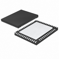
LTC2170IUKG-12#PBF Linear Technology, LTC2170IUKG-12#PBF Datasheet - Page 22

LTC2170IUKG-12#PBF
Manufacturer Part Number
LTC2170IUKG-12#PBF
Description
IC ADC 12BIT SER/PAR 25M 52-QFN
Manufacturer
Linear Technology
Datasheet
1.LTC2170CUKG-12PBF.pdf
(32 pages)
Specifications of LTC2170IUKG-12#PBF
Number Of Bits
12
Sampling Rate (per Second)
25M
Data Interface
Serial, Parallel
Number Of Converters
4
Power Dissipation (max)
238mW
Voltage Supply Source
Analog and Digital
Operating Temperature
-40°C ~ 85°C
Mounting Type
Surface Mount
Package / Case
52-WFQFN Exposed Pad
Lead Free Status / RoHS Status
Lead free / RoHS Compliant
Available stocks
Company
Part Number
Manufacturer
Quantity
Price
LTC2172-12/
LTC2171-12/LTC2170-12
APPLICATIONS INFORMATION
The differential encode mode is recommended for sinu-
soidal, PECL, or LVDS encode inputs (Figures 12 and 13).
The encode inputs are internally biased to 1.2V through
10k equivalent resistance. The encode inputs can be taken
above V
is from 1.1V to 1.6V. In the differential encode mode,
ENC
falsely triggering the single-ended encode mode. For
good jitter performance ENC
fall times.
The single-ended encode mode should be used with
CMOS encode inputs. To select this mode, ENC
nected to ground and ENC
encode input. ENC
so 1.8V to 3.3V CMOS logic levels can be used. The
ENC
ENC
Clock PLL and Duty Cycle Stabilizer
The encode clock is multiplied by an internal phase-locked
loop (PLL) to generate the serial digital output data. If the
encode signal changes frequency or is turned off, the PLL
requires 25μs to lock onto the input clock.
A clock duty cycle stabilizer circuit allows the duty cycle
of the applied encode signal to vary from 30% to 70%.
In the serial programming mode it is possible to disable
22
+
+
–
should have fast rise and fall times.
should stay at least 200mV above ground to avoid
threshold is 0.9V. For good jitter performance
T1 = MA/COM ETC1-1-13
RESISTORS AND CAPACITORS
ARE 0402 PACKAGE SIZE
DD
0.1μF
0.1μF
(up to 3.6V), and the common mode range
Figure 12. Sinusoidal Encode Drive
T1
+
50Ω
50Ω
can be taken above V
+
0.1μF
is driven with a square wave
+
should have fast rise and
100Ω
ENC
ENC –
+
DD
LTC2172-12
(up to 3.6V)
217212 F12
–
is con-
the duty cycle stabilizer, but this is not recommended. In
the parallel programming mode the duty cycle stabilizer
is always enabled.
DIGITAL OUTPUTS
The digital outputs of the LTC2172-12/LTC2171-12/
LTC2170-12 are serialized LVDS signals. Each channel
outputs two bits at a time (2-lane mode) or one bit at a
time (1-lane mode). The data can be serialized with 16-,
14-, or 12-bit serialization (see the Timing Diagrams sec-
tion for details).
The output data should be latched on the rising and falling
edges of the data clockout (DCO). A data frame output
(FR) can be used to determine when the data from a new
conversion result begins. In the 2-lane, 14-bit serialization
mode, the frequency of the FR output is halved.
The maximum serial data rate for the data outputs is
1Gbps, so the maximum sample rate of the ADC will de-
pend on the serialization mode as well as the speed grade
of the ADC (see Table 1). The minimum sample rate for
all serialization modes is 5Msps.
Figure 13. PECL or LVDS Encode Drive
PECL OR
CLOCK
LVDS
0.1μF
0.1μF
ENC
ENC
+
–
LTC2172-12
217212 F13
21721012f


