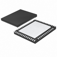
LTC2173CUKG-12#PBF Linear Technology, LTC2173CUKG-12#PBF Datasheet - Page 16

LTC2173CUKG-12#PBF
Manufacturer Part Number
LTC2173CUKG-12#PBF
Description
IC ADC 12BIT SER 80MSPS 52-QFN
Manufacturer
Linear Technology
Datasheet
1.LTC2173CUKG-12PBF.pdf
(32 pages)
Specifications of LTC2173CUKG-12#PBF
Number Of Bits
12
Sampling Rate (per Second)
80M
Data Interface
Serial, SPI™
Number Of Converters
4
Power Dissipation (max)
446mW
Voltage Supply Source
Single Supply
Operating Temperature
0°C ~ 70°C
Mounting Type
Surface Mount
Package / Case
52-WFQFN Exposed Pad
Lead Free Status / RoHS Status
Lead free / RoHS Compliant
Available stocks
Company
Part Number
Manufacturer
Quantity
Price
LTC2175-12/
LTC2174-12/LTC2173-12
PIN FUNCTIONS
A
Input.
A
Input.
V
Equal to V
mode of the analog inputs of channels 1 and 2. Bypass
to ground with a 0.1μF ceramic capacitor.
A
Input.
A
Input.
REFH (Pins 6,7): ADC High Reference. Bypass to pins 8, 9
with a 2.2μF ceramic capacitor and to ground with a 0.1μF
ceramic capacitor.
REFL (Pins 8,9): ADC Low Reference. Bypass to pins 6, 7
with a 2.2μF ceramic capacitor and to ground with a 0.1μF
ceramic capacitor.
A
Input.
A
Input.
V
Equal to V
mode of the analog inputs of channels 3 and 4. Bypass
to ground with a 0.1μF ceramic capacitor.
A
Input.
A
Input.
V
1.9V. Bypass to ground with 0.1μF ceramic capacitors.
Adjacent pins can share a bypass capacitor.
ENC
rising edge.
ENC
starts on the falling edge.
CS (Pin 19): In serial programming mode, (PAR/SER =
0V), CS is the serial interface chip select input. When CS
16
IN1
IN1
CM12
IN2
IN2
IN3
IN3
CM34
IN4
IN4
DD
+
–
+
–
+
+
–
–
+
–
(Pins 15, 16, 51, 52): Analog Power Supply, 1.7V to
(Pin 17): Encode Input. Conversion starts on the
(Pin 18): Encode Complement Input. Conversion
(Pin 2): Channel 1 Negative Differential Analog
(Pin 10): Channel 3 Positive Differential Analog
(Pin 11): Channel 3 Negative Differential Analog
(Pin 14): Channel 4 Negative Differential Analog
(Pin 1): Channel 1 Positive Differential Analog
(Pin 4): Channel 2 Positive Differential Analog
(Pin 5): Channel 2 Negative Differential Analog
(Pin 13): Channel 4 Positive Differential Analog
(Pin 12): Common Mode Bias Output, Nominally
(Pin 3): Common Mode Bias Output, Nominally
DD
DD
/2. V
/2. V
CM
CM
should be used to bias the common
should be used to bias the common
is low, SCK is enabled for shifting data on SDI into the
mode control registers. In the parallel programming mode
(PAR/SER = V
CS can be driven with 1.8V to 3.3V logic.
SCK (Pin 20): In serial programming mode, (PAR/SER =
0V), SCK is the serial interface clock input. In the parallel
programming mode (PAR/SER = V
or 1.75mA LVDS output currents. SCK can be driven with
1.8V to 3.3V logic.
SDI (Pin 21): In serial programming mode, (PAR/SER =
0V), SDI is the serial interface data Input. Data on SDI is
clocked into the mode control registers on the rising edge
of SCK. In the parallel programming mode (PAR/SER =
V
be driven with 1.8V to 3.3V logic.
GND (Pins 22, 45, 49, Exposed Pad Pin 53): ADC Power
Ground. The exposed pad must be soldered to the PCB
ground.
OGND (Pin 33): Output Driver Ground. Must be shorted
to the ground plane by a very low inductance path. Use
multiple vias close to the pin.
OV
to ground with a 0.1μF ceramic capacitor.
SDO (Pin 46): In serial programming mode, (PAR/SER
= 0V), SDO is the optional serial interface data output.
Data on SDO is read back from the mode control registers
and can be latched on the falling edge of SCK. SDO is an
open-drain NMOS output that requires an external 2k
pull-up resistor to 1.8V – 3.3V. If read back from the mode
control registers is not needed, the pull-up resistor is not
necessary and SDO can be left unconnected. In the parallel
programming mode (PAR/SER = V
enables internal 100Ω termination resistors on the digital
outputs. When used as an input, SDO can be driven with
1.8V to 3.3V logic through a 1k series resistor.
PAR/SER (Pin 47): Programming Mode Selection Pin.
Connect to ground to enable the serial programming mode.
CS, SCK, SDI, SDO become a serial interface that control
the A/D operating modes. Connect to V
parallel programming mode where CS, SCK, SDI, SDO
become parallel logic inputs that control a reduced set of
the A/D operating modes. PAR/SER should be connected
DD
DD
), SDI can be used to power down the part. SDI can
(Pin 34): Output Driver Supply, 1.7V to 1.9V. Bypass
DD
), CS selects 2-lane or 1-lane output mode.
DD
DD
), SDO is an input that
), SCK selects 3.5mA
DD
to enable the
21754312f


