LTC2173CUKG-12#PBF Linear Technology, LTC2173CUKG-12#PBF Datasheet - Page 19
LTC2173CUKG-12#PBF
Manufacturer Part Number
LTC2173CUKG-12#PBF
Description
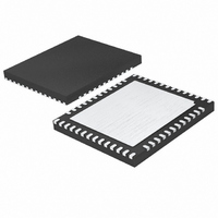
IC ADC 12BIT SER 80MSPS 52-QFN
Manufacturer
Linear Technology
Datasheet
1.LTC2173CUKG-12PBF.pdf
(32 pages)
Specifications of LTC2173CUKG-12#PBF
Number Of Bits
12
Sampling Rate (per Second)
80M
Data Interface
Serial, SPI™
Number Of Converters
4
Power Dissipation (max)
446mW
Voltage Supply Source
Single Supply
Operating Temperature
0°C ~ 70°C
Mounting Type
Surface Mount
Package / Case
52-WFQFN Exposed Pad
Lead Free Status / RoHS Status
Lead free / RoHS Compliant
Available stocks
Company
Part Number
Manufacturer
Quantity
Price


APPLICATIONS INFORMATION
CONVERTER OPERATION
The LTC2175-12/LTC2174-12/LTC2173-12 are low power,
4-channel, 12-bit, 125Msps/105Msps/80Msps A/D con-
verters that are powered by a single 1.8V supply. The
analog inputs should be driven differentially. The encode
input can be driven differentially for optimal jitter perfor-
mance, or single-ended for lower power consumption. The
digital outputs are serial LVDS to minimize the number
of data lines. Each channel outputs two bits at a time
(2-lane mode). At lower sampling rates there is a one bit
per channel option (1-lane mode). Many additional features
can be chosen by programming the mode control registers
through a serial SPI port.
ANALOG INPUT
The analog inputs are differential CMOS sample-and-hold
circuits (Figure 2). The inputs should be driven differen-
tially around a common mode voltage set by the V
or V
ENC
ENC
A
A
IN
IN
Figure 2. Equivalent Input Circuit. Only One of the Four
Analog Channels Is Shown.
+
–
+
–
CM34
LTC2175-12
10Ω
10Ω
output pins, which are nominally V
1.2V
1.2V
V
V
10k
10k
DD
DD
V
DD
C
1.8pF
C
1.8pF
PARASITIC
PARASITIC
25Ω
25Ω
R
R
ON
ON
DD
C
C
SAMPLE
SAMPLE
3.5pF
3.5pF
/2. For the
217512 F02
CM12
2V input range, the inputs should swing from V
to V
between the inputs.
The four channels are simultaneously sampled by a shared
encode circuit (Figure 2).
INPUT DRIVE CIRCUITS
Input Filtering
If possible, there should be an RC low pass fi lter right at
the analog inputs. This lowpass fi lter isolates the drive
circuitry from the A/D sample-and-hold switching, and
also limits wideband noise from the drive circuitry. Figure 3
shows an example of an input RC fi lter. The RC component
values should be chosen based on the application’s input
frequency.
Transformer Coupled Circuits
Figure 3 shows the analog input being driven by an RF
transformer with a center-tapped secondary. The center
Figure 3. Analog Input Circuit Using a Transformer.
Recommended for Input Frequencies from 5MHz to 70MHz.
ANALOG
CM
INPUT
LTC2174-12/LTC2173-12
+ 0.5V. There should be 180° phase difference
0.1μF
T1: MA/COM MABAES0060
RESISTORS, CAPACITORS
ARE 0402 PACKAGE SIZE
1:1
T1
25Ω
25Ω
0.1μF
50Ω
25Ω
25Ω
LTC2175-12/
0.1μF
12pF
V
A
A
CM
IN
IN
+
–
LTC2175-12
CM
217512 F03
19
– 0.5V
21754312f
Related parts for LTC2173CUKG-12#PBF
Image
Part Number
Description
Manufacturer
Datasheet
Request
R

Part Number:
Description:
IC ADC 12BIT 80MSPS QUAD 52QFN
Manufacturer:
Linear Technology
Datasheet:
Part Number:
Description:
IC ADC 14BIT 80MSPS QUAD 52QFN
Manufacturer:
Linear Technology
Datasheet:
Part Number:
Description:
IC ADC 14BIT SER 80MSPS 52-QFN
Manufacturer:
Linear Technology
Datasheet:

Part Number:
Description:
14-Bit, 125Msps/105Msps/80Msps Low Power Quad ADCs
Manufacturer:
LINER [Linear Technology]
Datasheet:

Part Number:
Description:
CD ROM LINEARVIEW DATASHEETS
Manufacturer:
Linear Technology

Part Number:
Description:
Standalone Linear Li-Ion Battery Charger with Thermal Regulation in ThinSOT
Manufacturer:
Linear Technology Corporation
Datasheet:
Part Number:
Description:
Low noise, high frequency, 8th order linear phase lowpass filter
Manufacturer:
Linear Technology Corporation
Datasheet:
Part Number:
Description:
Manufacturer:
Linear Technology Corporation
Datasheet:
Part Number:
Description:
Manufacturer:
Linear Technology Corporation
Datasheet:
Part Number:
Description:
Manufacturer:
Linear Technology Corporation
Datasheet:
Part Number:
Description:
Manufacturer:
Linear Technology Corporation
Datasheet:
Part Number:
Description:
Manufacturer:
Linear Technology Corporation
Datasheet:
Part Number:
Description:
Manufacturer:
Linear Technology Corporation
Datasheet:
Part Number:
Description:
Manufacturer:
Linear Technology Corporation
Datasheet:
Part Number:
Description:
Dual and Quad, JFET Input Precision High Speed Op Amps
Manufacturer:
Linear Technology Corporation
Datasheet: