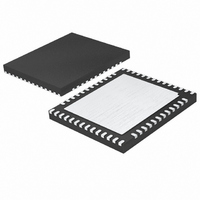
LTC2173CUKG-12#PBF Linear Technology, LTC2173CUKG-12#PBF Datasheet - Page 26

LTC2173CUKG-12#PBF
Manufacturer Part Number
LTC2173CUKG-12#PBF
Description
IC ADC 12BIT SER 80MSPS 52-QFN
Manufacturer
Linear Technology
Datasheet
1.LTC2173CUKG-12PBF.pdf
(32 pages)
Specifications of LTC2173CUKG-12#PBF
Number Of Bits
12
Sampling Rate (per Second)
80M
Data Interface
Serial, SPI™
Number Of Converters
4
Power Dissipation (max)
446mW
Voltage Supply Source
Single Supply
Operating Temperature
0°C ~ 70°C
Mounting Type
Surface Mount
Package / Case
52-WFQFN Exposed Pad
Lead Free Status / RoHS Status
Lead free / RoHS Compliant
Available stocks
Company
Part Number
Manufacturer
Quantity
Price
APPLICATIONS INFORMATION
LTC2175-12/
LTC2174-12/LTC2173-12
26
can be left fl oating and no pull-up resistor is needed. Table
4 shows a map of the mode control registers.
Software Reset
If serial programming is used, the mode control registers
should be programmed as soon as possible after the power
supplies turn on and are stable. The fi rst serial command
must be a software reset which will reset all register data
bits to logic 0. To perform a software reset, bit D7 in the
reset register is written with a logic 1. After the reset is
complete, bit D7 is automatically set back to zero.
GROUNDING AND BYPASSING
The LTC2175-12/LTC2174-12/LTC2173-12 requires a
printed circuit board with a clean unbroken ground plane.
A multilayer board with an internal ground plane in the
fi rst layer beneath the ADC is recommended. Layout for
the printed circuit board should ensure that digital and
analog signal lines are separated as much as possible. In
particular, care should be taken not to run any digital track
alongside an analog signal track or underneath the ADC.
High quality ceramic bypass capacitors should be used
at the V
Table 4. Serial Programming Mode Register Map (PAR/SER = GND)
REGISTER A0: RESET REGISTER (ADDRESS 00h)
REGISTER A1: FORMAT AND POWER-DOWN REGISTER (ADDRESS 01h)
Bit 7
Bits 6-0
Bit 7
Bit 6
Bit 5
DCSOFF
RESET
D7
D7
DD
, OV
RESET
0 = Not Used
1 = Software Reset. All Mode Control Registers are Reset to 00h. The ADC is Momentarily Placed in SLEEP Mode.
This Bit is Automatically Set Back to Zero After the Reset is Complete
Unused, Don’t Care Bits.
DCSOFF
0 = Clock Duty Cycle Stabilizer On
1 = Clock Duty Cycle Stabilizer Off. This is Not Recommended.
RAND
0 = Data Output Randomizer Mode Off
1 = Data Output Randomizer Mode On
TWOSCOMP
0 = Offset Binary Data Format
1 = Two’s Complement Data Format
DD
, V
RAND
D6
D6
X
CM
, V
Clock Duty Cycle Stabilizer Bit
Data Output Randomizer Mode Control Bit
Two’s Complement Mode Control Bit
REF
Software Reset Bit
, REFH and REFL pins.
TWOSCOMP
D5
D5
X
SLEEP
D4
D4
X
Bypass capacitors must be located as close to the pins as
possible. Of particular importance is the 0.1μF capacitor
between REFH and REFL. This capacitor should be on the
same side of the circuit board as the A/D, and as close to
the device as possible (1.5mm or less). Size 0402 ceramic
capacitors are recommended. The larger 2.2μF capacitor
between REFH and REFL can be somewhat further away.
The traces connecting the pins and bypass capacitors must
be kept short and should be made as wide as possible.
The analog inputs, encode signals, and digital outputs
should not be routed next to each other. Ground fi ll and
grounded vias should be used as barriers to isolate these
signals from each other.
HEAT TRANSFER
Most of the heat generated by the LTC2175-12/LTC2174-12/
LTC2173-12 is transferred from the die through the bot-
tom-side Exposed Pad and package leads onto the printed
circuit board. For good electrical and thermal performance,
the Exposed Pad must be soldered to a large grounded
pad on the PC board. This pad should be connected to
the internal ground planes by an array of vias.
NAP_4
D3
D3
X
NAP_3
D2
D2
X
NAP_2
D1
D1
X
NAP_1
D0
D0
X
21754312f


