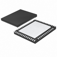
LTC2173CUKG-12#PBF Linear Technology, LTC2173CUKG-12#PBF Datasheet - Page 23

LTC2173CUKG-12#PBF
Manufacturer Part Number
LTC2173CUKG-12#PBF
Description
IC ADC 12BIT SER 80MSPS 52-QFN
Manufacturer
Linear Technology
Datasheet
1.LTC2173CUKG-12PBF.pdf
(32 pages)
Specifications of LTC2173CUKG-12#PBF
Number Of Bits
12
Sampling Rate (per Second)
80M
Data Interface
Serial, SPI™
Number Of Converters
4
Power Dissipation (max)
446mW
Voltage Supply Source
Single Supply
Operating Temperature
0°C ~ 70°C
Mounting Type
Surface Mount
Package / Case
52-WFQFN Exposed Pad
Lead Free Status / RoHS Status
Lead free / RoHS Compliant
Available stocks
Company
Part Number
Manufacturer
Quantity
Price
APPLICATIONS INFORMATION
DIGITAL OUTPUTS
The digital outputs of the LTC2175-12/LTC2174-12/
LTC2173-12 are serialized LVDS signals. Each channel
outputs two bits at a time (2-lane mode). At lower sam-
pling rates there is a one bit per channel option (1-lane
mode). The data can be serialized with 16, 14, or 12-bit
serialization (see timing diagrams for details).
The output data should be latched on the rising and falling
edges of the data clock out (DCO). A data frame output
(FR) can be used to determine when the data from a new
conversion result begins. In the 2-lane, 14-bit serialization
mode, the frequency of the FR output is halved.
The maximum serial data rate for the data outputs is
1Gbps, so the maximum sample rate of the ADC will de-
pend on the serialization mode as well as the speed grade
of the ADC (see Table 1). The minimum sample rate for all
serialization modes is 5Msps.
By default the outputs are standard LVDS levels: 3.5mA
output current and a 1.25V output common mode volt-
age. An external 100Ω differential termination resistor
is required for each LVDS output pair. The termination
resistors should be located as close as possible to the
LVDS receiver.
Table 1. Maximum Sampling Frequency for All Serialization Modes. Note That These Limits Are for the LTC2175-12. The Sampling
Frequency for the Slower Speed Grades Cannot Exceed 105MHz (LTC2174-12) or 80MHz (LTC2173-12).
SERIALIZATION MODE
2-Lane
2-Lane
2-Lane
1-Lane
1-Lane
1-Lane
16-Bit Serialization
14-Bit Serialization
12-Bit Serialization
16-Bit Serialization
14-Bit Serialization
12-Bit Serialization
MAXIMUM SAMPLING
FREQUENCY , f
62.5
71.4
83.3
125
125
125
S
(MHz)
DCO FREQUENCY
The outputs are powered by OV
isolated from the A/D core power and ground.
Programmable LVDS Output Current
The default output driver current is 3.5mA. This current
can be adjusted by control register A2 in the serial pro-
gramming mode. Available current levels are 1.75mA,
2.1mA, 2.5mA, 3mA, 3.5mA, 4mA and 4.5mA. In the
parallel programming mode the SCK pin can select either
3.5mA or 1.75mA.
Optional LVDS Driver Internal Termination
In most cases using just an external 100Ω termination
resistor will give excellent LVDS signal integrity. In addi-
tion, an optional internal 100Ω termination resistor can
be enabled by serially programming mode control register
A2. The internal termination helps absorb any refl ections
caused by imperfect termination at the receiver. When the
internal termination is enabled, the output driver current
is doubled to maintain the same output voltage swing.
In the parallel programming mode the SDO pin enables
internal termination. Internal termination should only be
used with 1.75mA, 2.1mA or 2.5mA LVDS output current
modes.
3.5 • f
4 • f
3 • f
8 • f
7 • f
6 • f
S
S
S
S
S
S
LTC2174-12/LTC2173-12
FR FREQUENCY
0.5 • f
f
f
f
f
f
S
S
S
S
S
S
LTC2175-12/
DD
and OGND which are
SERIAL DATA RATE
16 • f
14 • f
12 • f
8 • f
7 • f
6 • f
S
S
S
S
S
S
23
21754312f


