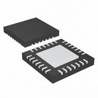
MAX1193ETI+ Maxim Integrated Products, MAX1193ETI+ Datasheet - Page 12

MAX1193ETI+
Manufacturer Part Number
MAX1193ETI+
Description
IC ADC 8BIT 45MSPS DUAL 28-TQFN
Manufacturer
Maxim Integrated Products
Datasheet
1.MAX1193ETI.pdf
(26 pages)
Specifications of MAX1193ETI+
Number Of Bits
8
Sampling Rate (per Second)
45M
Data Interface
Parallel
Number Of Converters
2
Voltage Supply Source
Single Supply
Operating Temperature
-40°C ~ 85°C
Mounting Type
Surface Mount
Package / Case
28-WFQFN Exposed Pad
Conversion Rate
45 MSPs
Resolution
8 bit
Snr
48.5 dB
Voltage Reference
1.024 V
Supply Voltage (max)
3.6 V
Supply Voltage (min)
2.7 V
Maximum Power Dissipation
1667 mW
Maximum Operating Temperature
+ 85 C
Mounting Style
SMD/SMT
Input Voltage
3 V
Minimum Operating Temperature
- 40 C
Lead Free Status / RoHS Status
Lead free / RoHS Compliant
Ultra-Low-Power, 45Msps, Dual 8-Bit ADC
12
(V
45.005678MHz at 50% duty cycle, T
DD
3, 5, 10
8, 9, 28
______________________________________________________________________________________
PIN
= 3.0V, OV
11
12
13
14
15
16
17
18
19
20
21
22
1
2
4
6
7
7
6
5
4
3
2
1
0
0
DIGITAL SUPPLY CURRENT
DD
OGND
NAME
OV
5
INA+
INB+
GND
INA-
CLK
INB-
vs. INPUT FREQUENCY
V
PD1
= 1.8V, V
ANALOG SUPPLY CURRENT
A/B
D7
D6
D5
D4
D3
D2
D1
D0
DD
SUPPLY CURRENT
DD
10
f
IN
(MHz)
REFIN
Channel A Negative Analog Input. For single-ended operation, connect INA- to COM.
Channel A Positive Analog Input. For single-ended operation, connect signal source to INA+.
Analog Ground. Connect all GND pins together.
Converter Clock Input
Channel B Positive Analog Input. For single-ended operation, connect signal source to INB+.
Channel B Negative Analog Input. For single-ended operation, connect INB- to COM.
Converter Power Input. Connect to a 2.7V to 3.6V power supply. Bypass V
combination of a 2.2µF capacitor in parallel with a 0.1µF capacitor.
Output Driver Ground
Output Driver Power Input. Connect to a 1.8V to V
combination of a 2.2µF capacitor in parallel with a 0.1µF capacitor.
Tri-State Digital Output. D7 is the most significant bit (MSB).
Tri-State Digital Output
Tri-State Digital Output
Tri-State Digital Output
Channel Data Indicator. This digital output indicates channel A data (A/B = 1) or channel B data
(A/B = 0) is present on the output.
Tri-State Digital Output
Tri-State Digital Output
Tri-State Digital Output
Tri-State Digital Output. D0 is the least significant bit (LSB).
Power-Down Digital Input 1. See Table 3.
15
A
= V
= +25°C, unless otherwise noted.)
20
MAX1193 toc29
DD
(internal reference), C
25
22.5
22.0
21.5
21.0
20.5
20.0
19.5
19.0
Typical Operating Characteristics (continued)
L
≈ 10pF at digital outputs, differential input at -0.5dB FS, f
A: ANALOG SUPPLY CURRENT (I
B: ANALOG SUPPLY CURRENT (I
C: DIGITAL SUPPLY CURRENT (I
FUNCTION
REFERENCE MODES
25
20
15
10
DD
5
0
0
power supply. Bypass OV
f
IN
= 11.531606MHz
10
vs. SAMPLING RATE
SUPPLY CURRENT
20
f
ODD
CLK
DD
DD
A
) - INTERNAL AND BUFFERED EXTERNAL
) - UNBUFFERED EXTERNAL REFERENCE MODE
) - ALL REFERENCE MODES
(MHz)
30
C
DD
Pin Description
B
to GND with a
40
DD
to GND with a
50
CLK
=


