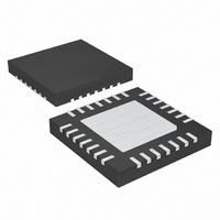
MAX1193ETI+ Maxim Integrated Products, MAX1193ETI+ Datasheet - Page 6

MAX1193ETI+
Manufacturer Part Number
MAX1193ETI+
Description
IC ADC 8BIT 45MSPS DUAL 28-TQFN
Manufacturer
Maxim Integrated Products
Datasheet
1.MAX1193ETI.pdf
(26 pages)
Specifications of MAX1193ETI+
Number Of Bits
8
Sampling Rate (per Second)
45M
Data Interface
Parallel
Number Of Converters
2
Voltage Supply Source
Single Supply
Operating Temperature
-40°C ~ 85°C
Mounting Type
Surface Mount
Package / Case
28-WFQFN Exposed Pad
Conversion Rate
45 MSPs
Resolution
8 bit
Snr
48.5 dB
Voltage Reference
1.024 V
Supply Voltage (max)
3.6 V
Supply Voltage (min)
2.7 V
Maximum Power Dissipation
1667 mW
Maximum Operating Temperature
+ 85 C
Mounting Style
SMD/SMT
Input Voltage
3 V
Minimum Operating Temperature
- 40 C
Lead Free Status / RoHS Status
Lead free / RoHS Compliant
ELECTRICAL CHARACTERISTICS (continued)
(V
0.33µF, T
Ultra-Low-Power, 45Msps, Dual 8-Bit ADC
Note 1: Specifications ≥+25°C guaranteed by production test, <+25°C guaranteed by design and characterization.
Note 2: SNR, SINAD, SFDR, HD3, and THD are based on a differential analog input voltage of -0.5dB FS referenced to the
Note 3: The power consumption of the output driver is proportional to the load capacitance (C L ).
Note 4: Guaranteed by design and characterization. Not production tested.
Note 5: SINAD settles to within 0.5dB of its typical value.
Note 6: Crosstalk rejection is measured by applying a high-frequency test tone to one channel and a low-frequency tone to the
Note 7: Amplitude/phase matching is measured by applying the same signal to each channel, and comparing the magnitude and
(V
45.005678MHz at 50% duty cycle, T
6
DD
DD
-10
-20
-30
-40
-50
-60
-70
-80
-90
_______________________________________________________________________________________
= 3.0V, OV
0
= 3.0V, OV
0
amplitude of the digital output. SNR and THD are calculated using HD2 through HD6.
second channel. FFTs are performed on each channel. The parameter is specified as power ratio of the first and second
channel FFT test tone bins.
phase of the fundamental bin on the calculated FFT.
FFT PLOT CHANNEL A (DIFFERENTIAL
f
f
f
A
A
INPUTS, 8192-POINT DATA RECORD)
CLK
INA
INB
INA
= -40°C to +85°C, unless otherwise noted. Typical values are at T
= 12.531448MHz
= 21.005678MHz
= 45.005678MHz
= A
ANALOG INPUT FREQUENCY (MHz)
INB
5
-10
-20
-30
-40
-50
-60
-70
-80
-90
DD
= -0.5dB FS
HD3
0
DD
0
= 1.8V, V
FFT PLOT CHANNEL B (DIFFERENTIAL
f
f
f
A
10
INPUTS, 8192-POINT DATA RECORD)
CLK
INA
INB
= 1.8V, V
INA
= 21.005678MHz
= 12.531448MHz
= 45.005678MHz
= A
ANALOG INPUT FREQUENCY (MHz)
INB
5
15
= -0.5dB FS
HD3
REFIN
REFIN
10
HD2
20
= V
f
INB
A
= V
= +25°C, unless otherwise noted.)
15
DD
25
DD
(internal reference), C
HD2
(internal reference), C
20
f
INA
-10
-20
-30
-40
-50
-60
-70
-80
-90
0
25
0
FFT PLOT CHANNEL B (DIFFERENTIAL
f
f
f
A
INPUTS, 8192-POINT DATA RECORD)
CLK
INA
INB
INA
HD2
= 12.531448MHz
= 21.005678MHz
= 45.005678MHz
= A
ANALOG INPUT FREQUENCY (MHz)
INB
5
= -0.5dB FS
L
10
≈ 10pF at digital outputs, f
L
≈ 10pF at digital outputs, differential input at -0.5dB FS, f
f
INA
Typical Operating Characteristics
15
HD3
A
=+25°C.) (Note 1)
20
25
-10
-20
-30
-40
-50
-60
-70
-80
-90
0
0
TWO-TONE IMD PLOT (DIFFERENTIAL
INPUTS, 8192-POINT DATA RECORD)
CLK
ANALOG INPUT FREQUENCY (MHz)
-10
-20
-30
-40
-50
-60
-70
-80
-90
f
IN1
f
IN2
5
0
= 45MHz, C
0
FFT PLOT CHANNEL A (DIFFERENTIAL
f
f
f
A
INPUTS, 8192-POINT DATA RECORD)
CLK
INA
INB
INA
HD2
10
= 21.005678MHz
= 12.531448MHz
= 45.005678MHz
= A
ANALOG INPUT FREQUENCY (MHz)
INB
5
= -0.5dB FS
f
f
f
A
CLK
IN1
IN2
IN
15
REFP
= 7dB FS
= 1.8MHz
= 2.3MHz
= 45.005678MHz
10
= C
f
INB
20
15
REFN
HD3
25
= C
20
COM
CLK
25
=
=


