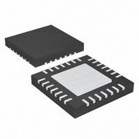
MAX1193ETI+ Maxim Integrated Products, MAX1193ETI+ Datasheet - Page 19

MAX1193ETI+
Manufacturer Part Number
MAX1193ETI+
Description
IC ADC 8BIT 45MSPS DUAL 28-TQFN
Manufacturer
Maxim Integrated Products
Datasheet
1.MAX1193ETI.pdf
(26 pages)
Specifications of MAX1193ETI+
Number Of Bits
8
Sampling Rate (per Second)
45M
Data Interface
Parallel
Number Of Converters
2
Voltage Supply Source
Single Supply
Operating Temperature
-40°C ~ 85°C
Mounting Type
Surface Mount
Package / Case
28-WFQFN Exposed Pad
Conversion Rate
45 MSPs
Resolution
8 bit
Snr
48.5 dB
Voltage Reference
1.024 V
Supply Voltage (max)
3.6 V
Supply Voltage (min)
2.7 V
Maximum Power Dissipation
1667 mW
Maximum Operating Temperature
+ 85 C
Mounting Style
SMD/SMT
Input Voltage
3 V
Minimum Operating Temperature
- 40 C
Lead Free Status / RoHS Status
Lead free / RoHS Compliant
Figure 8. Transformer-Coupled Input Drive
An RF transformer (Figure 8) provides an excellent
solution to convert a single-ended source signal to a
fully differential signal, required by the MAX1193 for
optimum performance. Connecting the center tap of the
transformer to COM provides a V
the input. Although a 1:1 transformer is shown, a step-
up transformer can be selected to reduce the drive
requirements. A reduced signal swing from the input
driver, such as an op amp, can also improve the overall
distortion.
In general, the MAX1193 provides better SFDR and
THD with fully differential input signals than single-
ended drive, especially for high input frequencies. In
differential input mode, even-order harmonics are lower
as both inputs (INA+, INA- and/or INB+, INB-) are bal-
V
V
IN
IN
N.C.
N.C.
0.1µF
0.1µF
MINICIRCUITS
MINICIRCUITS
3
3
1
2
1
2
TT1-6-KK81
TT1-6-KK81
T1
T1
Ultra-Low-Power, 45Msps, Dual 8-Bit ADC
6
5
4
6
5
4
______________________________________________________________________________________
Using Transformer Coupling
2.2µF
2.2µF
25Ω
25Ω
25Ω
25Ω
0.1µF
0.1µF
22pF
22pF
22pF
22pF
DD
/2 DC level shift to
INA+
COM
INA-
INB+
INB-
MAX1193
anced, and each of the ADC inputs only requires half
the signal swing compared to single-ended mode.
Figure 9 shows an AC-coupled, single-ended applica-
tion. Amplifiers such as the MAX4108 provide high
speed, high bandwidth, low noise, and low distortion to
maintain the input signal integrity.
The buffered external reference mode allows for more
control over the MAX1193 reference voltage and allows
multiple converters to use a common reference. To
drive one MAX1193 in buffered external reference
mode, the external circuit must sink 0.7µA, allowing one
reference circuit to easily drive the REFIN of multiple
converters to 1.024V ±10%.
Figure 9. Using an Op Amp for Single-Ended, AC-Coupled
Input Drive
V
V
IN
IN
MAX4108
MAX4108
Single-Ended AC-Coupled Input Signal
Buffered External Reference Drives
100Ω
100Ω
100Ω
100Ω
0.1µF
0.1µF
REFP
REFN
REFP
REFN
1kΩ
1kΩ
1kΩ
1kΩ
R
50Ω
R
50Ω
0.1µF
0.1µF
ISO
ISO
22pF
22pF
22pF
22pF
R
50Ω
C
50Ω
C
C
R
C
ISO
IN
IN
ISO
IN
IN
Multiple ADCs
INA+
COM
INA-
INB+
INB-
MAX1193
19


