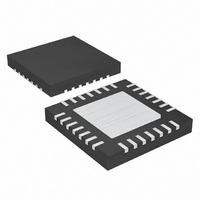
MAX1193ETI+ Maxim Integrated Products, MAX1193ETI+ Datasheet - Page 4

MAX1193ETI+
Manufacturer Part Number
MAX1193ETI+
Description
IC ADC 8BIT 45MSPS DUAL 28-TQFN
Manufacturer
Maxim Integrated Products
Datasheet
1.MAX1193ETI.pdf
(26 pages)
Specifications of MAX1193ETI+
Number Of Bits
8
Sampling Rate (per Second)
45M
Data Interface
Parallel
Number Of Converters
2
Voltage Supply Source
Single Supply
Operating Temperature
-40°C ~ 85°C
Mounting Type
Surface Mount
Package / Case
28-WFQFN Exposed Pad
Conversion Rate
45 MSPs
Resolution
8 bit
Snr
48.5 dB
Voltage Reference
1.024 V
Supply Voltage (max)
3.6 V
Supply Voltage (min)
2.7 V
Maximum Power Dissipation
1667 mW
Maximum Operating Temperature
+ 85 C
Mounting Style
SMD/SMT
Input Voltage
3 V
Minimum Operating Temperature
- 40 C
Lead Free Status / RoHS Status
Lead free / RoHS Compliant
ELECTRICAL CHARACTERISTICS (continued)
(V
0.33µF, T
Ultra-Low-Power, 45Msps, Dual 8-Bit ADC
4
Maximum REFP/REFN/COM Sink
Current
REFIN Input Resistance
REFIN Input Current
REFP Input Voltage
REFN Input Voltage
COM Input Voltage
Differential Reference Input
Voltage
REFP Input Resistance
REFN Input Resistance
DIGITAL INPUTS (CLK, PD0, PD1)
Input High Threshold
Input Low Threshold
Input Hysteresis
Digital Input Leakage Current
Digital Input Capacitance
DIGITAL OUTPUTS (D7–D0, A/B)
Output Voltage Low
Output Voltage High
Tri-State Leakage Current
Tri-State Output Capacitance
POWER REQUIREMENTS
Analog Supply Voltage
Digital Output Supply Voltage
UNBUFFERED EXTERNAL REFERENCE (REFIN = GND, V
DD
_______________________________________________________________________________________
= 3.0V, OV
A
= -40°C to +85°C, unless otherwise noted. Typical values are at T
PARAMETER
DD
= 1.8V, V
REFIN
= V
SYMBOL
R
R
V
V
OV
I
C
DD
DC
I
V
V
LEAK
SINK
DI
V
V
HYST
REFN
V
COM
REFP
V
OUT
REF
OL
OH
DD
IH
IL
IN
DD
IN
(internal reference), C
V
V
V
Measured between REFP and COM
Measured between REFN and COM
CLK
PD0, PD1
CLK
PD0, PD1
CLK at GND or V
PD0 and PD1 at OGND or OV
I
I
SINK
SOURCE
REFP
REFN
REFP
= 200µA
- V
- V
- V
= 200µA
COM
REFN
COM
REFP
CONDITIONS
L
DD
≈ 10pF at digital outputs, f
, V
REFN
, and V
A
DD
= +25°C.) (Note 1)
COM
are applied externally)
CLK
OV
OV
0.7 x
0.7 x
0.8 x
MIN
V
2.7
1.8
DD
DD
DD
= 45MHz, C
V
-0.256
0.256
0.512
>500
DD
TYP
-0.7
0.1
3.0
2
4
4
5
5
/ 2
REFP
= C
OV
OV
MAX
0.3 x
0.3 x
0.2 x
V
V
±5
±5
±5
3.6
DD
DD
REFN
DD
DD
= C
UNITS
mA
COM
kΩ
µA
kΩ
kΩ
µA
pF
µA
pF
V
V
V
V
V
V
V
V
V
V
V
=


