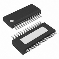
MAX1295ACEI+ Maxim Integrated Products, MAX1295ACEI+ Datasheet

MAX1295ACEI+
Specifications of MAX1295ACEI+
Related parts for MAX1295ACEI+
MAX1295ACEI+ Summary of contents
Page 1
... MAX1297BCEG 0°C to +70°C MAX1297AEEG -40°C to +85°C MAX1297BEEG -40°C to +85°C ________________________________________________________________ Maxim Integrated Products For pricing, delivery, and ordering information, please contact Maxim/Dallas Direct! at 1-888-629-4642, or visit Maxim’s website at www.maxim-ic.com. ♦ 12-Bit Resolution, ±0.5 LSB Linearity ♦ +3V Single-Supply Operation ♦ ...
Page 2
ADCs with +2.5V Reference and Parallel Interface ABSOLUTE MAXIMUM RATINGS V to GND ..............................................................-0.3V to +6V DD CH0–CH5, COM to GND ............................-0. REF, REFADJ to GND.................................-0. Digital Inputs to GND ...............................................-0.3V to ...
Page 3
ADCs with +2.5V Reference and Parallel Interface ELECTRICAL CHARACTERISTICS (continued +2.7V to +3.6V, COM = GND, REFADJ = unless otherwise noted. Typical values are at T ...
Page 4
ADCs with +2.5V Reference and Parallel Interface TIMING CHARACTERISTICS (V = +2.7V to +3.6V, COM = GND, REFADJ = unless otherwise noted. Typical values are ...
Page 5
ADCs with +2.5V Reference and Parallel Interface (V = +3V +2.500V 4.8MHz REF CLK INTEGRAL NONLINEARITY vs. DIGITAL OUTPUT CODE 0.5 0.4 0.3 0.2 0.1 0 -0.1 -0.2 -0.3 -0.4 ...
Page 6
ADCs with +2.5V Reference and Parallel Interface (V = +3V +2.500V 4.8MHz REF CLK INTERNAL REFERENCE VOLTAGE vs. SUPPLY VOLTAGE 2.53 2.52 2.51 2.50 2.49 2.48 3.0 3.3 2.7 3.6 ...
Page 7
ADCs with +2.5V Reference and Parallel Interface PIN NAME MAX1295 MAX1297 ...
Page 8
ADCs with +2.5V Reference and Parallel Interface PIN NAME MAX1295 MAX1297 25 21 REF D11 28 24 D10 (CH5) (CH4) ANALOG INPUT (CH3) MULTIPLEXER (CH2) CH1 CH0 COM CLK CLOCK ...
Page 9
ADCs with +2.5V Reference and Parallel Interface the analog inputs. This configuration is pseudo-differ- ential in that only the signal at IN+ is sampled. The return side (IN-) must remain stable within ±0.5 LSB (±0.1 LSB ...
Page 10
ADCs with +2.5V Reference and Parallel Interface Table 2. Channel Selection for Single-Ended Operation *Channels ...
Page 11
ADCs with +2.5V Reference and Parallel Interface CSWS CONTROL D7–D0 BYTE ACQMOD = "0" HIGH-Z INT RD HIGH-Z DOUT Figure 4. Conversion Timing Using Internal Acquisition Mode ...
Page 12
ADCs with +2.5V Reference and Parallel Interface CSWS CONTROL D7–D0 BYTE ACQMOD = "1" HIGH-Z INT RD HIGH-Z DOUT Figure 5. Conversion Timing Using External Acquisition Mode ...
Page 13
ADCs with +2.5V Reference and Parallel Interface CLK t CWS WR ACQMOD = "0" t ACQUISITION STARTS CWH CLK WR ACQMOD = "0" WR Timing (Internal Acquisition Mode) Figure 6a. External Clock and ACQUISITION STARTS CLK ...
Page 14
ADCs with +2.5V Reference and Parallel Interface Table 4. Control-Byte Format D7 D6 (MSB) PD1 PD0 ACQMOD V = +3V DD 50kΩ 330kΩ 50kΩ GND 0.01µF 4.7µF GND Figure 7. Reference Adjustment with External Potentiometer the ...
Page 15
ADCs with +2.5V Reference and Parallel Interface Table 5. Full-Scale and Zero-Scale for Unipolar and Bipolar Operation UNIPOLAR MODE Zero Scale Full Scale OUTPUT CODE FULL-SCALE TRANSITION FS = REF + COM 111 . . . ...
Page 16
ADCs with +2.5V Reference and Parallel Interface ; ; ; ; CLK WR RD CONTROL D11– D7–D0 WORD D0 STATE ACQUISITION SAMPLING INSTANT Figure 10. Timing Diagram for Fastest Conversion SUPPLIES ...
Page 17
ADCs with +2.5V Reference and Parallel Interface Integral Nonlinearity Integral nonlinearity (INL) is the deviation of the values on an actual transfer function from a straight line. This straight line can be either a best-straight-line fit ...
Page 18
ADCs with +2.5V Reference and Parallel Interface CLK MAX1295 REF µP WR REFADJ CONTROL INPUTS RD INT D11 D10 CH5 D6 CH4 D5 CH3 D4 CH2 D3 CH1 D2 CH0 ...
Page 19
... Maxim cannot assume responsibility for use of any circuitry other than circuitry entirely embodied in a Maxim product. No circuit patent licenses are implied. Maxim reserves the right to change the circuitry and specifications without notice at any time. Maxim Integrated Products, 120 San Gabriel Drive, Sunnyvale, CA 94086 408-737-7600 ____________________19 © 2002 Maxim Integrated Products Printed USA is a registered trademark of Maxim Integrated Products ...


