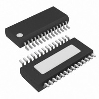
MAX1295ACEI+ Maxim Integrated Products, MAX1295ACEI+ Datasheet - Page 4

MAX1295ACEI+
Manufacturer Part Number
MAX1295ACEI+
Description
IC ADC 12BIT 265KSPS 28-QSOP
Manufacturer
Maxim Integrated Products
Datasheet
1.MAX1297BEEG.pdf
(19 pages)
Specifications of MAX1295ACEI+
Number Of Bits
12
Sampling Rate (per Second)
265k
Data Interface
Parallel
Number Of Converters
1
Power Dissipation (max)
762mW
Voltage Supply Source
Single Supply
Operating Temperature
0°C ~ 70°C
Mounting Type
Surface Mount
Package / Case
28-QSOP
Lead Free Status / RoHS Status
Lead free / RoHS Compliant
TIMING CHARACTERISTICS
(V
T
265ksps, +3V, 6-/2-Channel, 12-Bit ADCs
with +2.5V Reference and Parallel Interface
4
Note 1: Tested at V
Note 2: Relative accuracy is the deviation of the analog value at any code from its theoretical value after offset and gain errors have
Note 3: Offset nulled.
Note 4: On channel is grounded; sine wave applied to off channels.
Note 5: Conversion time is defined as the number of clock cycles times the clock period; clock has a 50% duty cycle.
Note 6: Input voltage range referenced to negative input. The absolute range for the analog inputs is from GND to V
Note 7: External load should not change during conversion for specified accuracy.
Note 8: When bit 5 is set low for internal acquisition, WR must not return low until after the first falling clock edge of the conversion.
Figure 1. Load Circuits for Enable/Disable Times
A
CLK Period
CLK Pulse Width High
CLK Pulse Width Low
Data Valid to WR Rise Time
WR Rise to Data Valid Hold Time
WR to CLK Fall Setup Time
CLK Fall to WR Hold Time
CS to CLK or WR Setup Time
CLK or WR to CS Hold Time
CS Pulse Width
WR Pulse Width (Note 8)
CS Rise to Output Disable
RD Rise to Output Disable
RD Fall to Output Data Valid
RD Fall to INT High Delay
CS Fall to Output Data Valid
DD
DOUT
= T
a) HIGH-Z TO V
_______________________________________________________________________________________
= +2.7V to +3.6V, COM = GND, REFADJ = V
MIN
6kΩ
been removed.
PARAMETER
to T
MAX
OH
AND V
, unless otherwise noted. Typical values are at T
DD
OL
= +3V, COM = GND, unipolar single-ended input mode.
TO V
C
20pF
LOAD
OH
SYMBOL
b) HIGH-Z TO V
DOUT
t
t
t
t
CSWS
CSWH
t
t
CWH
CWS
t
t
t
t
INT1
DO2
t
t
t
t
t
t
WR
DO
CP
CH
DS
DH
CS
CL
TC
TR
V
C
C
C
C
C
OL
DD
LOAD
LOAD
LOAD
LOAD
LOAD
3kΩ
AND V
C
20pF
DD
LOAD
, V
OH
= 20pF, Figure 1
= 20pF, Figure 1
= 20pF, Figure 1
= 20pF, Figure 1
= 20pF, Figure 1
TO V
REF
OL
= +2.5V, 4.7µF capacitor at REF pin, f
CONDITIONS
A
= +25°C.)
MIN
208
100
40
40
40
40
40
60
60
20
20
20
0
0
CLK
= 4.8MHz (50% duty cycle),
TYP
DD
MAX
100
100
110
70
70
.
UNITS
ns
ns
ns
ns
ns
ns
ns
ns
ns
ns
ns
ns
ns
ns
ns
ns


