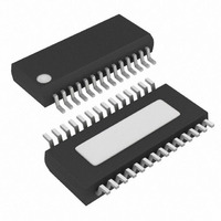
MAX1295ACEI+ Maxim Integrated Products, MAX1295ACEI+ Datasheet - Page 8

MAX1295ACEI+
Manufacturer Part Number
MAX1295ACEI+
Description
IC ADC 12BIT 265KSPS 28-QSOP
Manufacturer
Maxim Integrated Products
Datasheet
1.MAX1297BEEG.pdf
(19 pages)
Specifications of MAX1295ACEI+
Number Of Bits
12
Sampling Rate (per Second)
265k
Data Interface
Parallel
Number Of Converters
1
Power Dissipation (max)
762mW
Voltage Supply Source
Single Supply
Operating Temperature
0°C ~ 70°C
Mounting Type
Surface Mount
Package / Case
28-QSOP
Lead Free Status / RoHS Status
Lead free / RoHS Compliant
265ksps, +3V, 6-/2-Channel, 12-Bit ADCs
with +2.5V Reference and Parallel Interface
The MAX1295/MAX1297 ADCs use a successive-
approximation (SAR) conversion technique and an input
track/hold (T/H) stage to convert an analog input signal
to a 12-bit digital output. This output format provides an
easy interface to standard microprocessors (µPs). Figure
2 shows the simplified internal architecture of the
MAX1295/MAX1297.
8
Figure 2. Simplified Functional Diagram of 6-/2-Channel MAX1295/MAX1297
_______________Detailed Description
MAX1295
_______________________________________________________________________________________
25
26
27
28
(CH5)
(CH4)
(CH3)
(CH2)
COM
CH1
CH0
CLK
WR
INT
( ) ARE FOR MAX1295 ONLY.
CS
RD
PIN
MAX1297
21
22
23
24
CLOCK
MULTIPLEXER
ANALOG
INPUT
NAME
Converter Operation
CONTROL LOGIC
REF
V
D11
D10
DD
LATCHES
&
Bandgap Reference Buffer Output/External Reference Input. Add a 4.7µF capacitor
to GND when using the internal reference.
Analog +2.7V to +3.6V Power Supply. Bypass with a 0.1µF capacitor to GND.
Three-State Digital Output (D11)
Three-State Digital Output (D10)
REF
T/H
12
CHARGE REDISTRIBUTION
THREE-STATE, BIDIRECTIONAL
12-BIT DAC
I/O INTERFACE
The sampling architecture of the ADC’s analog com-
parator is illustrated in the equivalent input circuit in
Figure 3. In single-ended mode, IN+ is internally
switched to channels CH0–CH5 for the MAX1295
(Figure 3a) and to CH0–CH1 for the MAX1297 (Figure
3b), while IN- is switched to COM (Table 2). In differen-
tial mode, IN+ and IN- are selected from analog input
pairs (Table 3) and are internally switched to either of
APPROXIMATION
SUCCESSIVE-
12-BIT DATA BUS
REGISTER
D0–D11
12
A
2.05
V
FUNCTION
=
Pin Description (continued)
MAX1295
MAX1297
REFADJ
Pseudo-Differential Operation
COMP
17kΩ
REFERENCE
1.22V
Single-Ended and
V
GND
DD


