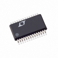
LTC1405IGN Linear Technology, LTC1405IGN Datasheet - Page 10

LTC1405IGN
Manufacturer Part Number
LTC1405IGN
Description
IC ADC 12BIT 5MSPS SAMPLE 28SSOP
Manufacturer
Linear Technology
Datasheet
1.LTC1405IGNPBF.pdf
(20 pages)
Specifications of LTC1405IGN
Number Of Bits
12
Sampling Rate (per Second)
5M
Data Interface
Parallel
Number Of Converters
1
Power Dissipation (max)
145mW
Voltage Supply Source
Dual ±
Operating Temperature
-40°C ~ 85°C
Mounting Type
Surface Mount
Package / Case
28-SSOP (0.150", 3.95mm Width)
Lead Free Status / RoHS Status
Contains lead / RoHS non-compliant
Available stocks
Company
Part Number
Manufacturer
Quantity
Price
Part Number:
LTC1405IGN
Manufacturer:
LINEAR/凌特
Quantity:
20 000
Company:
Part Number:
LTC1405IGN#PBF
Manufacturer:
Linear Technology
Quantity:
135
Part Number:
LTC1405IGN#PBF
Manufacturer:
LINEAR/凌特
Quantity:
20 000
Part Number:
LTC1405IGN#TRPBF
Manufacturer:
LINEAR/凌特
Quantity:
20 000
APPLICATIO S I FOR ATIO
LTC1405
An external reference or a DAC can be used to drive V
over a 0V to 5V range (Figures 3a and 3b). The input
impedance of the V
required for high accuracy. Driving V
useful in applications where the peak input signal ampli-
tude may vary. The input span of the ADC can then be
adjusted to match the peak input signal, maximizing the
signal-to-noise ratio.
Both the V
capacitors to ground. For best performance, 1µF or larger
ceramic capacitors are recommended. For the case of
external circuitry driving V
used at V
this case, a 0.05µF or larger ceramic capacitor is accept-
able.
The V
can be used by external circuitry. For single 5V supply
applications it is convenient to connect A
V
Driving the Analog Inputs
The differential inputs of the LTC1405 are easy to drive.
The inputs may be driven differentially or single-ended
(i. e., the A
A
mode signal is reduced by the high common mode rejec-
tion of the sample-and-hold circuit. Any common mode
input value is acceptable as long as the input pins stay
between V
inputs are high impedance. At the end of conversion the
inputs draw a small current spike while charging the
sample-and-hold.
For superior dynamic performance in dual supply mode,
the LTC1405 should be operated with the analog inputs
centered at ground, and in single supply mode the inputs
should be centered at 2.5V. If required, the analog inputs
can be driven differentially via a transformer. Refer to
Table 2 for a summary of the analog input and reference
configurations and their relative advantages.
10
CM
IN
+
pin.
inputs are simultaneously sampled and any common
CM
pin is a low output impedance 2.5V reference that
REF
IN
DD
CM
so the input range can be changed quickly. In
–
input is held at a fixed value). The A
and V
and V
U
REF
SS
REF
. During conversion the analog
pin is 2kΩ, so a buffer may be
U
pins must be bypassed with
REF
, a smaller capacitor can be
W
REF
IN
–
with a DAC is
directly to the
U
IN
–
and
REF
SENSE
V
V
REF
CM
1µF
1µF
LTC1450
Figure 3a. Using the LT1019-2.5 As an
External Reference; Input Range = ±1.25V
LT1019A-2.5
Figure 3b. Driving V
R1
10k
R2
10k
V
5V
Figure 2. Reference Circuit
IN
V
OUT
5k
5k
REFERENCE
LOGIC
2.5V
1µF
1µF
1µF
1µF
5V
REF
LTC1405
V
SENSE
V
with a DAC
REF
CM
V
SENSE
V
REF
CM
LTC1405
+
–
1405 F03a
+
–
2.048V
1405 F02
2.048V
2k
1405 F03b
1405fa
TO
ADC


