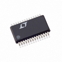
LTC1405IGN Linear Technology, LTC1405IGN Datasheet - Page 7

LTC1405IGN
Manufacturer Part Number
LTC1405IGN
Description
IC ADC 12BIT 5MSPS SAMPLE 28SSOP
Manufacturer
Linear Technology
Datasheet
1.LTC1405IGNPBF.pdf
(20 pages)
Specifications of LTC1405IGN
Number Of Bits
12
Sampling Rate (per Second)
5M
Data Interface
Parallel
Number Of Converters
1
Power Dissipation (max)
145mW
Voltage Supply Source
Dual ±
Operating Temperature
-40°C ~ 85°C
Mounting Type
Surface Mount
Package / Case
28-SSOP (0.150", 3.95mm Width)
Lead Free Status / RoHS Status
Contains lead / RoHS non-compliant
Available stocks
Company
Part Number
Manufacturer
Quantity
Price
Part Number:
LTC1405IGN
Manufacturer:
LINEAR/凌特
Quantity:
20 000
Company:
Part Number:
LTC1405IGN#PBF
Manufacturer:
Linear Technology
Quantity:
135
Part Number:
LTC1405IGN#PBF
Manufacturer:
LINEAR/凌特
Quantity:
20 000
Part Number:
LTC1405IGN#TRPBF
Manufacturer:
LINEAR/凌特
Quantity:
20 000
+ A
– A
V
mon mode for single supply operation. Bypass to GND
with a 1µF to 10µF ceramic.
SENSE (Pin 4): Reference Programming Pin. Ground
selects V
SENSE to V
V
10µF ceramic.
GND (Pin 6): DAC Reference Ground.
V
to 10µF ceramic.
GND (Pin 8): Analog Power Ground.
D11 to D0 (Pins 9 to 20): Data Outputs. The output format
is two’s complement.
PI FU CTIO S
CM
REF
DD
IN
IN
U
(Pin 7): Analog 5V Supply. Bypass to GND with a 1µF
(Pin 3): 2.5V Reference Output.Optional input com-
(Pin 5): DAC Reference. Bypass to GND with a 1µF to
(Pin 1): Positive Analog Input.
(Pin 2): Negative Analog Input.
REF
U
DD
= 4.096V. Short to V
to drive V
U
REF
with an external reference.
REF
for 2.048V. Connect
OGND (Pin 21): Output Logic Ground. Tie to GND.
OV
Connect to Pin 23 for 5V logic. If not shorted to Pin 23,
bypass to GND with a 1µF ceramic.
V
ceramic.
GND (Pin 24): Analog Power Ground.
V
not shorted to GND, bypass to GND with a 1µF ceramic.
CLK (Pin 26): Conversion Start Signal. This active high
signal starts a conversion on its rising edge.
OF (Pin 27): Overflow Output. This signal is high when the
digital output is 011111111111 or 100000000000.
GAIN (Pin 28): Gain Select for Input PGA. 5V selects an
input gain of 1, 0V selects a gain of 2.
DD
SS
DD
(Pin 25): Negative Supply. Can be – 5V or 0V. If V
(Pin 23): Analog 5V Supply. Bypass to GND with a 1µF
(Pin 22): Positive Supply for the Output Logic.
LTC1405
SS
1405fa
7
is


