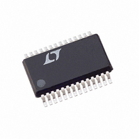
LTC1405IGN Linear Technology, LTC1405IGN Datasheet - Page 14

LTC1405IGN
Manufacturer Part Number
LTC1405IGN
Description
IC ADC 12BIT 5MSPS SAMPLE 28SSOP
Manufacturer
Linear Technology
Datasheet
1.LTC1405IGNPBF.pdf
(20 pages)
Specifications of LTC1405IGN
Number Of Bits
12
Sampling Rate (per Second)
5M
Data Interface
Parallel
Number Of Converters
1
Power Dissipation (max)
145mW
Voltage Supply Source
Dual ±
Operating Temperature
-40°C ~ 85°C
Mounting Type
Surface Mount
Package / Case
28-SSOP (0.150", 3.95mm Width)
Lead Free Status / RoHS Status
Contains lead / RoHS non-compliant
Available stocks
Company
Part Number
Manufacturer
Quantity
Price
Part Number:
LTC1405IGN
Manufacturer:
LINEAR/凌特
Quantity:
20 000
Company:
Part Number:
LTC1405IGN#PBF
Manufacturer:
Linear Technology
Quantity:
135
Part Number:
LTC1405IGN#PBF
Manufacturer:
LINEAR/凌特
Quantity:
20 000
Part Number:
LTC1405IGN#TRPBF
Manufacturer:
LINEAR/凌特
Quantity:
20 000
APPLICATIO S I FOR ATIO
LTC1405
are present. The SNR performance of an ADC when the
performance is limited by jitter is given by:
where f
the root-mean-square jitter due to the clock, the analog
input and the A/D aperture jitter. To minimize clock jitter,
use a clean clock source such as a crystal oscillator, treat
the clock signals as sensitive analog traces and use
dedicated packages with good supply bypassing for any
clock drivers.
Board Layout
To obtain the best performance from the LTC1405, a
printed circuit board with a ground plane is required.
Layout for the printed circuit board should ensure that
digital and analog signal lines are separated as much as
possible. In particular, care should be taken not to run any
digital track alongside an analog signal track.
An analog ground plane separate from the logic system
ground should be placed under and around the ADC.
Pins 6, 8 and 24 (GND), Pin 21 (OGND) and all other
analog grounds should be connected to this ground plane.
In single supply mode, Pin 25 (V
14
CIRCUITRY
ANALOG
INPUT
IN
SNR = – 20log (2π f
is the frequency of an input sine wave and t
+
–
1000pF
U
1
+A
2
IN
U
–A
IN
BYPASS CAPACITORS
PLACE NON-GROUND
GROUND PLANE AND
IN
t
VIAS AWAY FROM
J
)dB
V
CM
Figure 13. Cross Section of LTC1405 Printed Circuit Board
3
W
1µF
SS
) should also be
V
REF
5
1µF
Figure 12. Power Supply Grounding
ANALOG GROUND PLANE
GND
U
6
AVOID BREAKING GROUND PLANE
J
V
DD
is
7
1µF
LTC1405
IN THIS AREA
LTC1405
GND
connected to this ground plane. All bypass capacitors for
the LTC1405 should also be connected to this ground
plane (Figure 12). The digital system ground should be
connected to the analog ground plane at only one point,
near the OGND pin.
The analog ground plane should be as close to the ADC as
possible. Care should be taken to avoid making holes in the
analog ground plane under and around the part. To ac-
complish this, we recommend placing vias for power and
signal traces outside the area containing the part and the
decoupling capacitors (Figure 13).
Supply Bypassing
High quality, low series resistance ceramic 1µF capacitors
should be used at both V
connected to – 5V it should also be bypassed to ground
with 1µF. In single supply operation V
to the ground plane as close to the part as possible. If OV
is not shorted to Pin 23 (V
decoupling capacitor to ground. Surface mount capaci-
tors such as the AVX 0805ZC105KAT provide excellent
bypassing in a small board space. The traces connecting
the pins and the bypass capacitors must be kept short and
should be made as wide as possible.
8
V
DD
23
1µF
OV
DD
22
1µF
GND
BYPASS
CAPACITOR
ANALOG
GROUND
PLANE
24
1405 F13
DD
pins, V
V
SS
DD
25
1µF
) it also requires a 1µF
OGND
CM
SS
21
and V
should be shorted
REF
SYSTEM
DIGITAL
. If V
1405 F12
SS
1405fa
DD
is


