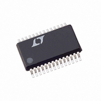
LTC1405IGN Linear Technology, LTC1405IGN Datasheet - Page 4

LTC1405IGN
Manufacturer Part Number
LTC1405IGN
Description
IC ADC 12BIT 5MSPS SAMPLE 28SSOP
Manufacturer
Linear Technology
Datasheet
1.LTC1405IGNPBF.pdf
(20 pages)
Specifications of LTC1405IGN
Number Of Bits
12
Sampling Rate (per Second)
5M
Data Interface
Parallel
Number Of Converters
1
Power Dissipation (max)
145mW
Voltage Supply Source
Dual ±
Operating Temperature
-40°C ~ 85°C
Mounting Type
Surface Mount
Package / Case
28-SSOP (0.150", 3.95mm Width)
Lead Free Status / RoHS Status
Contains lead / RoHS non-compliant
Available stocks
Company
Part Number
Manufacturer
Quantity
Price
Part Number:
LTC1405IGN
Manufacturer:
LINEAR/凌特
Quantity:
20 000
Company:
Part Number:
LTC1405IGN#PBF
Manufacturer:
Linear Technology
Quantity:
135
Part Number:
LTC1405IGN#PBF
Manufacturer:
LINEAR/凌特
Quantity:
20 000
Part Number:
LTC1405IGN#TRPBF
Manufacturer:
LINEAR/凌特
Quantity:
20 000
TI I G CHARACTERISTICS
LTC1405
temperature range, otherwise specifications are at T
operation. (Note 5)
SYMBOL
I
C
V
V
I
I
POWER REQUIRE E TS
range, otherwise specifications are at T
(Note 5)
SYMBOL
V
V
I
I
P
range, otherwise specifications are at T
(Note 5)
SYMBOL
f
t
t
t
t
t
Note 1: Absolute Maximum Ratings are those values beyond which the life
of a device may be impaired.
Note 2: All voltage values are with respect to ground with GND and OGND
wired together (unless otherwise noted).
Note 3: When these pin voltages are taken below V
will be clamped by internal diodes. This product can handle input currents
greater than 100mA below V
DIGITAL I PUTS AND OUTPUTS
4
IN
SOURCE
SINK
DD
SS
SAMPLE
CONV
ACQ
H
L
AD
IN
OH
OL
DD
SS
D
W U
PARAMETER
Digital Input Current
Digital Input Capacitance
High Level Output Voltage
Low Level Output Voltage
Output Source Current
Output Sink Current
PARAMETER
Positive Supply Voltage
Negative Supply Voltage
Positive Supply Current
Negative Supply Current
Power Dissipation
PARAMETER
Sampling Frequency
Conversion Time
Acquisition Time
CLK High Time
CLK Low Time
Aperture Delay of Sample-and-Hold
U
SS
or above V
W U
U
DD
without latchup.
A
A
= 25°C. Specifications are guaranteed for both dual supply and single supply operation.
= 25°C. Specifications are guaranteed for both dual supply and single supply operation.
SS
or above V
The
●
A
CONDITIONS
V
0V
0V
0V
0V
0V
0V
0V
0V
V
V
CONDITIONS
(Note 10)
Dual Supply Mode
Single Supply Mode
The
CONDITIONS
(Note 9)
(Note 9)
IN
OUT
OUT
= 25°C. Specifications are guaranteed for both dual supply and single supply
denotes the specifications which apply over the full operating temperature
DD
DD
DD
DD
DD
DD
DD
DD
= 0V to V
DD
●
= 0V
= V
= 4.75V, I
= 4.75V, I
= 2.7V, I
= 2.7V, I
= 4.75V, I
= 4.75V, I
= 2.7V, I
= 2.7V, I
, they
The
denotes the specifications which apply over the full operating temperature
DD
●
DD
O
O
O
O
denotes the specifications which apply over the full operating
O
O
O
O
= –10µA
= –200µA
= 160µA
= 1.6mA
= –10µA
= –200µA
= 160µA
= 1.6mA
Note 4: When these pin voltages are taken below V
by internal diodes. This product can handle input currents greater than
100mA below V
is taken above V
can handle input currents of greater than 100mA above V
latchup.
Note 5: V
otherwise specified.
DD
= 5V, V
SS
DD
without latchup. GAIN is not clamped to V
, it will be clamped by an internal diode. The CLK pin
SS
= – 5V or 0V, f
●
●
●
●
●
●
●
●
●
●
●
●
●
– 5.25
4.75
0.02
SAMPLE
MIN
MIN
MIN
4.0
2.3
20
20
20
= 5MHz, t
– 250
4.74
4.71
0.05
0.10
0.05
0.10
TYP
TYP
TYP
115
150
100
100
1.8
2.6
0.8
50
50
35
23
0
SS
they will be clamped
r
= t
DD
– 4.75
MAX
MAX
MAX
f
5.25
±10
145
180
0.4
0.4
1.2
28
= 5ns unless
5
without
DD
. When CLK
UNITS
UNITS
UNITS
1405fa
MHz
mW
mA
mA
mA
mA
µA
pF
ns
ns
ns
ns
ps
V
V
V
V
V
V
V
V
V
V
V


