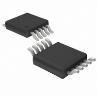
LTC2411-1IMS#TR Linear Technology, LTC2411-1IMS#TR Datasheet - Page 10

LTC2411-1IMS#TR
Manufacturer Part Number
LTC2411-1IMS#TR
Description
IC A/DCONV DIFF INPUT&REF 10MSOP
Manufacturer
Linear Technology
Datasheet
1.LTC2411CMSPBF.pdf
(40 pages)
Specifications of LTC2411-1IMS#TR
Number Of Bits
24
Sampling Rate (per Second)
6.8
Data Interface
MICROWIRE™, Serial, SPI™
Number Of Converters
2
Power Dissipation (max)
1mW
Voltage Supply Source
Single Supply
Operating Temperature
-40°C ~ 85°C
Mounting Type
Surface Mount
Package / Case
10-TFSOP, 10-MSOP (0.118", 3.00mm Width)
Lead Free Status / RoHS Status
Contains lead / RoHS non-compliant
Other names
LTC2411-1IMSTR
LTC24111IMSTR
LTC24111IMSTR
Available stocks
Company
Part Number
Manufacturer
Quantity
Price
PI FU CTIO S
LTC2411/LTC2411-1
the Sleep mode and remains in this low power state as
long as CS is HIGH. A LOW-to-HIGH transition on CS
during the Data Output transfer aborts the data transfer
and starts a new conversion.
SDO (Pin 8): Three-State Digital Output. During the Data
Output period, this pin is used as the serial data output.
When the chip select CS is HIGH (CS = V
is in a high impedance state. During the Conversion and
Sleep periods, this pin is used as the conversion status
output. The conversion status can be observed by pulling
CS LOW.
SCK (Pin 9): Bidirectional Digital Clock Pin. In Internal
Serial Clock Operation mode, SCK is used as the digital
output for the internal serial interface clock during the Data
Output period. In External Serial Clock Operation mode,
SCK is used as the digital input for the external serial
interface clock during the Data Output period. A weak
FU CTIO AL BLOCK DIAGRA
TEST CIRCUITS
10
U
U
REF
REF
GND
V
IN
IN
CC
+
–
+
–
U
U
+
–
U
SDO
– +
DAC
Hi-Z TO V
V
V
1.69k
OL
OH
TO V
TO Hi-Z
OH
OH
2411 TA03
CC
C
LOAD
), the SDO pin
= 20pF
W
Figure 1
internal pull-up is automatically activated in Internal Serial
Clock Operation mode. The Serial Clock Operation mode is
determined by the logic level applied to the SCK pin at
power up or during the most recent falling edge of CS.
F
controls the ADC’s notch frequencies and conversion
time. For the LTC2411, when the F
(F
digital filter first null is located at 50Hz. When the F
connected to GND (F
oscillator and the digital filter first null is located at 60Hz.
For the LTC2411-1, the converter provides simultaneous
50Hz/60Hz rejection with the F
When F
frequency f
system clock and the digital filter first null is located at a
frequency f
O
O
ADC
(Pin 10): Frequency Control Pin. Digital input that
= V
CC
O
), the converter uses its internal oscillator and the
is driven by an external clock signal with a
EOSC
EOSC
SDO
/2560.
, the converters use this signal as their
AUTOCALIBRATION
DECIMATING FIR
Hi-Z TO V
V
V
AND CONTROL
OH
OL
O
V
TO Hi-Z
TO V
CC
= OV), the converter uses its internal
1.69k
2411 TA04
OL
C
OL
LOAD
= 20pF
O
O
pin connected to GND.
OSCILLATOR
INTERFACE
INTERNAL
pin is connected to V
SERIAL
(INT/EXT)
F
SDO
SCK
CS
2411 FD
O
O
pin is
CC


