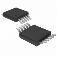
LTC2411-1IMS#TR Linear Technology, LTC2411-1IMS#TR Datasheet - Page 34

LTC2411-1IMS#TR
Manufacturer Part Number
LTC2411-1IMS#TR
Description
IC A/DCONV DIFF INPUT&REF 10MSOP
Manufacturer
Linear Technology
Datasheet
1.LTC2411CMSPBF.pdf
(40 pages)
Specifications of LTC2411-1IMS#TR
Number Of Bits
24
Sampling Rate (per Second)
6.8
Data Interface
MICROWIRE™, Serial, SPI™
Number Of Converters
2
Power Dissipation (max)
1mW
Voltage Supply Source
Single Supply
Operating Temperature
-40°C ~ 85°C
Mounting Type
Surface Mount
Package / Case
10-TFSOP, 10-MSOP (0.118", 3.00mm Width)
Lead Free Status / RoHS Status
Contains lead / RoHS non-compliant
Other names
LTC2411-1IMSTR
LTC24111IMSTR
LTC24111IMSTR
Available stocks
Company
Part Number
Manufacturer
Quantity
Price
APPLICATIO S I FOR ATIO
LTC2411/LTC2411-1
the sensor largely eliminates the need for protection
devices, RFI suppression and wiring. The LTC2411/
LTC2411-1 exhibit extremely low temperature dependent
drift. As a result, exposure to external ambient tempera-
ture ranges does not compromise performance. The in-
corporation of any amplification considerably complicates
thermal stability, as input offset voltages and currents,
temperature coefficient of gain settling resistors all be-
come factors.
The circuit in Figure 41 shows an example of a simple
amplification scheme. This example produces a differen-
tial output with a common mode voltage of 2.5V, as
determined by the bridge. The use of a true three amplifier
instrumentation amplifier is not necessary, as the LTC2411/
LTC2411-1 have common mode rejection far beyond that
of most amplifiers. The LTC1051 is a dual autozero ampli-
fier that can be used to produce a gain of 30 before its input
referred noise dominates the LTC2411/LTC2411-1 noise.
This example shows a gain of 34, that is determined by a
feedback network built using a resistor array containing
eight individual resistors. The resistors are organized to
optimize temperature tracking in the presence of thermal
gradients. The second LTC1051 buffers the low noise
34
BRIDGE
350
U
RN1
RN1 = 5k 8 RESISTOR ARRAY
U1A, U1B, U2A, U2B = 1/2 LTC1051
U
16
1
Figure 41. Using Autozero Amplifiers to Reduce Input Referred Noise
6
3
2
6
5
W
11
–
+
+
–
15
2
U1A
U1B
5V
4
7
8
10
14
0.1 F
3
U
1
7
8
9
13
4
5
input stage from the transient load steps produced during
conversion.
The gain stability and accuracy of this approach is very
good, due to a statistical improvement in resistor match-
ing due to individual error contribution being reduced. A
gain of 34 may seem low, when compared to common
practice in earlier generations of load-cell interfaces, how-
ever the accuracy of the LTC2411/LTC2411-1 changes the
rationale. Achieving high gain accuracy and linearity at
higher gains may prove difficult, while providing little
benefit in terms of noise reduction.
At a gain of 100, the gain error that could result from
typical open-loop gain of 160dB is –1ppm, however,
worst-case is at the minimum gain of 116dB, giving a gain
error of –158ppm. Worst-case gain error at a gain of 34,
is –54ppm. The use of the LTC1051A reduces the worst-
case gain error to –33ppm. The advantage of gain higher
than 34, then becomes dubious, as the input referred
noise sees little improvement
tially compromised.
1
0.048 V
Input referred noise for A
12
RMS
.
2
3
6
5
–
+
–
+
U2A
U2B
5V
V
4
8
= 34 is approximately 0.05 V
0.1 F
1
7
2
3
4
5
1
REF
REF
IN
IN
and gain accuracy is poten-
LTC2411-1
+
–
LTC2411/
+
–
GND
RMS
V
CC
6
, whereas at a gain of 50, it would be
1
SDO
SCK
CS
F
5V
0.1 F
O
REF
8
9
7
10
2411 F41


