LTC2411-1IMS#TR Linear Technology, LTC2411-1IMS#TR Datasheet - Page 21

LTC2411-1IMS#TR
Manufacturer Part Number
LTC2411-1IMS#TR
Description
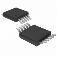
IC A/DCONV DIFF INPUT&REF 10MSOP
Manufacturer
Linear Technology
Datasheet
1.LTC2411CMSPBF.pdf
(40 pages)
Specifications of LTC2411-1IMS#TR
Number Of Bits
24
Sampling Rate (per Second)
6.8
Data Interface
MICROWIRE™, Serial, SPI™
Number Of Converters
2
Power Dissipation (max)
1mW
Voltage Supply Source
Single Supply
Operating Temperature
-40°C ~ 85°C
Mounting Type
Surface Mount
Package / Case
10-TFSOP, 10-MSOP (0.118", 3.00mm Width)
Lead Free Status / RoHS Status
Contains lead / RoHS non-compliant
Other names
LTC2411-1IMSTR
LTC24111IMSTR
LTC24111IMSTR
Available stocks
Company
Part Number
Manufacturer
Quantity
Price
APPLICATIO S I FOR ATIO
The internal serial clock mode is selected at the end of the
power-on reset (POR) cycle. The POR cycle is concluded
approximately 1ms after V
weak pull-up is active during the POR cycle; therefore, the
internal serial clock timing mode is automatically selected
if SCK is not externally driven LOW (if SCK is loaded such
that the internal pull-up cannot pull the pin HIGH, the
external SCK mode will be selected).
During the conversion, the SCK and the serial data output
pin (SDO) are HIGH (EOC = 1). Once the conversion is
complete, SCK and SDO go LOW (EOC = 0) indicating the
conversion has finished and the device has entered the
low power sleep state. The part remains in the sleep state
a minimum amount of time (1/2 the internal SCK period)
then immediately begins outputting data. The data output
cycle begins on the first rising edge of SCK and ends after
the 32nd rising edge. Data is shifted out the SDO pin on
each falling edge of SCK. The internally generated serial
clock is output to the SCK pin. This signal may be used
to shift the conversion result into external circuitry. EOC
can be latched on the first rising edge of SCK and the last
bit of the conversion result can be latched on the 32nd
rising edge of SCK. After the 32nd rising edge, SDO goes
HIGH (EOC = 1) indicating a new conversion is in progress.
SCK remains HIGH during the conversion.
PRESERVING THE CONVERTER ACCURACY
The LTC2411/LTC2411-1 are designed to reduce as much
as possible the conversion result sensitivity to device
decoupling, PCB layout, antialiasing circuits, line fre-
quency perturbations and so on. Nevertheless, in order to
preserve the extreme accuracy capability of this part,
some simple precautions are desirable.
Digital Signal Levels
The LTC2411/LTC2411-1’s digital interface is easy to use.
Its digital inputs (F
operation) accept standard TTL/CMOS logic levels and the
internal hysteresis receivers can tolerate edge rates as slow
as 100 s. However, some considerations are required to
take advantage of the exceptional accuracy and low supply
current of this converter.
O
U
, CS and SCK in External SCK mode of
U
CC
exceeds 1.9V. An internal
W
U
The digital output signals (SDO and SCK in Internal SCK
mode of operation) are less of a concern because they are
not generally active during the conversion state.
While a digital input signal is in the range 0.5V to
(V
current from the power supply. It should be noted that,
when any one of the digital input signals (F
in External SCK mode of operation) is within this range,
the LTC2411/LTC2411-1 power supply current may in-
crease even if the signal in question is at a valid logic level.
For micropower operation, it is recommended to drive all
digital input signals to full CMOS levels [V
V
During the conversion period, the undershoot and/or
overshoot of a fast digital signal connected to the LTC2411/
LTC2411-1 pins may severely disturb the analog to digital
conversion process. Undershoot and overshoot can oc-
cur because of the impedance mismatch at the converter
pin when the transition time of an external control signal
is less than twice the propagation delay from the driver to
LTC2411/LTC2411-1. For reference, on a regular FR-4
board, signal propagation velocity is approximately
183ps/inch for internal traces and 170ps/inch for surface
traces. Thus, a driver generating a control signal with a
minimum transition time of 1ns must be connected to the
converter pin through a trace shorter than 2.5 inches. This
problem becomes particularly difficult when shared con-
trol lines are used and multiple reflections may occur. The
solution is to carefully terminate all transmission lines
close to their characteristic impedance.
Parallel termination near the LTC2411/LTC2411-1 pin will
eliminate this problem but will increase the driver power
dissipation. A series resistor between 27
placed near the driver or near the LTC2411/LTC2411-1 pin
will also eliminate this problem without additional power
dissipation. The actual resistor value depends upon the
trace impedance and connection topology.
An alternate solution is to reduce the edge rate of the
control signals. It should be noted that using very slow
edges will increase the converter power supply current
during the transition time. The differential input and refer-
ence architecture reduce substantially the converter’s
sensitivity to ground currents.
OH
CC
> (V
– 0.5V), the CMOS input receiver draws additional
CC
– 0.4V)].
LTC2411/LTC2411-1
O
IL
, CS and SCK
< 0.4V and
and 56
21


