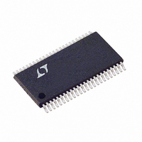
LTC1851CFW Linear Technology, LTC1851CFW Datasheet - Page 18

LTC1851CFW
Manufacturer Part Number
LTC1851CFW
Description
IC ADC 12BIT 1.25MSPS 48-TSSOP
Manufacturer
Linear Technology
Datasheet
1.LTC1851CFWPBF.pdf
(28 pages)
Specifications of LTC1851CFW
Number Of Bits
12
Sampling Rate (per Second)
1.25M
Data Interface
Parallel
Number Of Converters
1
Power Dissipation (max)
50mW
Voltage Supply Source
Single Supply
Operating Temperature
0°C ~ 70°C
Mounting Type
Surface Mount
Package / Case
48-TFSOP (0.240", 6.10mm Width)
Lead Free Status / RoHS Status
Contains lead / RoHS non-compliant
Available stocks
Company
Part Number
Manufacturer
Quantity
Price
Company:
Part Number:
LTC1851CFW
Manufacturer:
ABOV
Quantity:
270
Part Number:
LTC1851CFW
Manufacturer:
LT/凌特
Quantity:
20 000
Company:
Part Number:
LTC1851CFW#PBF
Manufacturer:
AD
Quantity:
21
APPLICATIO S I FOR ATIO
LTC1850/LTC1851
BOARD LAYOUT AND BYPASSING
To obtain the best performance from the LTC1850/
LTC1851, a printed circuit board with ground plane is
required. The ground plane under the ADC area should be
18
1111...1111
1111...1110
1111...1101
1000...0001
1000...0000
0111...1111
0111...1110
0000...0010
0000...0001
0000...0000
0111...1111
0111...1110
0111...1101
0000...0001
0000...0000
1111...1111
1111...1110
1000...0010
1000...0001
1000...0000
DIFFERENTIAL BIT
SINGLE-ENDED/
Bipolar Transfer Characteristic
(UNI/BIP = 1)
Unipolar Transfer Characteristic
(UNI/BIP = 0)
S6
Figure 1. Readback Status Word
– FS
0
S5
A2
MUX ADDRESS
U
INPUT VOLTAGE (V)
INPUT VOLTAGE (V)
S4
A1
–1LSB 0 1LSB
BIPOLAR
U
ZERO
S3
A0
BIPOLAR BIT
UNIPOLAR/
FS =
FS = V
S2
V
W
PGA BIT
REFCOMP
REFCOMP
S1
FS – 1LSB
2
FS – 1LSB
SEQUENCE BIT
1851 F01A
1851 F01B
END OF
S0
1851 F01
U
as free of breaks and holes as possible, such that a low
impedance path between all ADC grounds and all ADC
decoupling capacitors is provided. It is critical to prevent
digital noise from being coupled to the analog inputs,
reference or analog power supply lines. Layout for the
printed circuit board should ensure that digital and analog
signal lines are separated as much as possible. In particu-
lar, care should be taken not to run any digital track
alongside an analog signal track or underneath the ADC.
An analog ground plane separate from the logic system
ground should be established under and around the ADC.
Pin 34 (OGND), Pin 13 (GND), Pin 16 (ADC’s GND) and all
other analog grounds should be connected to this single
analog ground point. The bypass capacitors should also
be connected to this analog ground plane. No other digital
grounds should be connected to this analog ground plane.
In some applications, it may be desirable to connect the
OV
system ground. In these cases, OV
to OGND instead of the analog ground plane.
Low impedance analog and digital power supply common
returns are essential to the low noise operation of the ADC
and the foil width for these tracks should be as wide as
possible. In applications where the ADC data outputs and
control signals are connected to a continuously active
microprocessor bus, it is possible to get errors in the
conversion results. These errors are due to feedthrough
from the microprocessor to the successive approximation
comparator. The problem can be eliminated by forcing the
microprocessor into a WAIT state during conversions or
by using three-state buffers to isolate the ADC bus. The
traces connecting the pins and bypass capacitors must be
kept short and should be made as wide as possible.
The LTC1850/LTC1851 have differential inputs to mini-
mize noise coupling. Common mode noise on the “+” and
“–” inputs will be rejected by the input CMRR. The LTC1850/
LTC1851 will hold and convert the difference between
whichever input is selected as the “+” input and whichever
input is selected as the “–” input. Leads to the inputs
should be kept as short as possible.
DD
to the logic system supply and OGND to the logic
DD
should be bypassed
18501f


