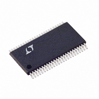
LTC1851CFW Linear Technology, LTC1851CFW Datasheet - Page 20

LTC1851CFW
Manufacturer Part Number
LTC1851CFW
Description
IC ADC 12BIT 1.25MSPS 48-TSSOP
Manufacturer
Linear Technology
Datasheet
1.LTC1851CFWPBF.pdf
(28 pages)
Specifications of LTC1851CFW
Number Of Bits
12
Sampling Rate (per Second)
1.25M
Data Interface
Parallel
Number Of Converters
1
Power Dissipation (max)
50mW
Voltage Supply Source
Single Supply
Operating Temperature
0°C ~ 70°C
Mounting Type
Surface Mount
Package / Case
48-TFSOP (0.240", 6.10mm Width)
Lead Free Status / RoHS Status
Contains lead / RoHS non-compliant
Available stocks
Company
Part Number
Manufacturer
Quantity
Price
Company:
Part Number:
LTC1851CFW
Manufacturer:
ABOV
Quantity:
270
Part Number:
LTC1851CFW
Manufacturer:
LT/凌特
Quantity:
20 000
Company:
Part Number:
LTC1851CFW#PBF
Manufacturer:
AD
Quantity:
21
APPLICATIO S I FOR ATIO
LTC1850/LTC1851
Figures 5 through 9 show several different modes of
operation. In modes 1a and 1b (Figures 5 and 6),
CS and RD are both tied low. The falling edge of
CONVST starts the conversion. The data outputs are
always enabled and data can be latched with the
BUSY rising edge. Mode 1a shows operation with a narrow
logic low CONVST pulse. Mode 1b shows a narrow logic
high CONVST pulse.
20
CS = RD = LOW
CONVST
BUSY
DATA
U
CS = RD = LOW
Figure 5. Mode 1a CONVST Starts a Conversion. Data Outputs Always Enabled
U
CONVST
Figure 6. Mode 1b CONVST Starts a Conversion. Data is Read by RD
BUSY
DATA
t
13
W
DATA (N – 1)
t
6
t
6
DATA (N – 1)
t
5
U
t
t
CONV
CONV
t
5
t
7
t
7
In mode 2 (Figure 7), CS is tied low. The falling edge of
CONVST signal again starts the conversion. Data outputs
are in three-state until read by the MPU with the
RD signal. Mode 2 can be used for operation with a shared
MPU databus.
In slow memory and ROM modes (Figures 8 and 9), CS is
tied low and CONVST and RD are tied together. The MPU
starts the conversion and reads the output with the RD
signal. Conversions are started by the MPU or DSP (no
external sample clock).
t
8
t
8
DATA N
DATA N
t
6
1851 F05
1851 F06
18501f


