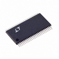
LTC1851CFW Linear Technology, LTC1851CFW Datasheet - Page 19

LTC1851CFW
Manufacturer Part Number
LTC1851CFW
Description
IC ADC 12BIT 1.25MSPS 48-TSSOP
Manufacturer
Linear Technology
Datasheet
1.LTC1851CFWPBF.pdf
(28 pages)
Specifications of LTC1851CFW
Number Of Bits
12
Sampling Rate (per Second)
1.25M
Data Interface
Parallel
Number Of Converters
1
Power Dissipation (max)
50mW
Voltage Supply Source
Single Supply
Operating Temperature
0°C ~ 70°C
Mounting Type
Surface Mount
Package / Case
48-TFSOP (0.240", 6.10mm Width)
Lead Free Status / RoHS Status
Contains lead / RoHS non-compliant
Available stocks
Company
Part Number
Manufacturer
Quantity
Price
Company:
Part Number:
LTC1851CFW
Manufacturer:
ABOV
Quantity:
270
Part Number:
LTC1851CFW
Manufacturer:
LT/凌特
Quantity:
20 000
Company:
Part Number:
LTC1851CFW#PBF
Manufacturer:
AD
Quantity:
21
APPLICATIO S I FOR ATIO
SUPPLY BYPASSING
High quality, low series resistance ceramic 10 F bypass
capacitors should be used. Surface mount ceramic ca-
pacitors provide excellent bypassing in a small board
space. Alternatively, 10 F tantalum capacitors in parallel
with 0.1 F ceramic capacitors can be used. Bypass ca-
pacitors must be located as close to the pins as possible.
The traces connecting the pins and the bypass capacitors
must be kept short and should be made as wide as
possible.
DIGITAL INTERFACE
Internal Clock
The A/D converter has an internal clock that eliminates the
need of synchronization between the external clock and
the CS and RD signals found in other ADCs. The internal
clock is factory trimmed to achieve a typical conversion
time of 550ns, and a maximum conversion time over the
full operating temperature range of 650ns. No external
adjustments are required. The guaranteed maximum ac-
quisition time is 150ns. In addition, a throughput time of
800ns and a minimum sampling rate of 1.25Msps is
guaranteed.
Figure 3. SHDN to CONVST Wake-Up Timing
CONVST
Figure 2. CS to SHDN Timing
SHDN
SHDN
CS
U
U
t
t
4
3
W
1851 F02
1851 F03
U
Power Shutdown
The LTC1850/LTC1851 provide two power shutdown
modes, Nap and Sleep, to save power during inactive
periods. The Nap mode reduces the power to 5mW and
leaves only the digital logic and reference powered up. The
wake-up time from Nap to active is 200ns. In Sleep mode,
all bias currents are shut down and only leakage current
remains—about 50 A. Wake-up time from sleep mode is
much slower since the reference circuit must power-up
and settle to 0.005% for full 12-bit accuracy (0.02% for full
10-bit accuracy). Sleep mode wake-up time is dependent
on the value of the capacitor connected to the REFCOMP
(Pin 12). The wake-up time is 10ms with the recom-
mended 10 F capacitor.
Shutdown is controlled by Pin 47 (SHDN); the ADC is in
shutdown when it is low. The shutdown mode is selected
with Pin 46 (CS); low selects Nap.
Timing and Control
Conversion start and data read operations are controlled
by three digital inputs: CONVST, CS and RD. A transition
from 1 to 0 applied to the CONVST pin will start a
conversion after the ADC has been selected (i.e., CS is
low). Once initiated, it cannot be restarted until the conver-
sion is complete. Converter status is indicated by the
BUSY output. BUSY is low during a conversion. If CONVST
returns high at a critical point during the conversion it can
create small errors. For the best results, ensure that
CONVST returns high either within 400ns after the start of
the conversion or after BUSY rises.
Figure 4. CS to CONVST Setup Timing
CONVST
RD
CS
LTC1850/LTC1851
t
1
t
2
1851 F04
19
18501f


