LTC1851CFW Linear Technology, LTC1851CFW Datasheet - Page 6
LTC1851CFW
Manufacturer Part Number
LTC1851CFW
Description
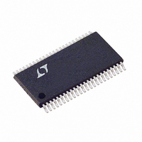
IC ADC 12BIT 1.25MSPS 48-TSSOP
Manufacturer
Linear Technology
Datasheet
1.LTC1851CFWPBF.pdf
(28 pages)
Specifications of LTC1851CFW
Number Of Bits
12
Sampling Rate (per Second)
1.25M
Data Interface
Parallel
Number Of Converters
1
Power Dissipation (max)
50mW
Voltage Supply Source
Single Supply
Operating Temperature
0°C ~ 70°C
Mounting Type
Surface Mount
Package / Case
48-TFSOP (0.240", 6.10mm Width)
Lead Free Status / RoHS Status
Contains lead / RoHS non-compliant
Available stocks
Company
Part Number
Manufacturer
Quantity
Price
Company:

Part Number:
LTC1851CFW
Manufacturer:
ABOV
Quantity:
270
Part Number:
LTC1851CFW
Manufacturer:
LT/凌特
Quantity:
20 000
Company:
Part Number:
LTC1851CFW#PBF
Manufacturer:
AD
Quantity:
21


LTC1850/LTC1851
TI I G CHARACTERISTICS
range, otherwise specifications are at T
SYMBOL
t
t
t
t
t
t
t
t
t
t
t
6
Note 1: Absolute maximum ratings are those values beyond which the life
of a device may be impaired.
Note 2: All voltage values are with respect to ground with GND, OGND and
GND wired together unless otherwise noted.
Note 3: When these pin voltages are taken below ground or above V
they will be clamped by internal diodes. This product can handle input
currents of 100mA below ground or above V
Note 4: When these pin voltages are taken below ground, they will be
clamped by internal diodes. This product can handle input currents of
100mA below ground without latchup. These pins are not clamped to V
Note 5: V
otherwise specified.
Note 6: Linearity, offset and full-scale specifications apply for a single-
ended input on any channel with COM grounded.
17
18
19
20
21
22
23
24
25
26
27
W
DD
U
= 4.75V to 5.25V, f
PARAMETER
WR High Time
M1 to M0 Setup Time
M0 to BUSY Delay
M0 to WR (or RD) Setup Time
M0 High Pulse Width
RD High Time Between Readback Reads
Last WR (or RD) to M0
M0 to RD Setup Time
M0 to CONVST
Aperture Delay
Aperture Jitter
SAMPLE
= 1.25MHz, t
DD
A
= 25 C. (Note 5)
without latchup.
r
= t
f
= 2ns unless
The
CONDITIONS
(Note 10)
(Notes 9, 10)
M1 High
(Notes 9, 10)
(Note 10)
(Note 10)
(Note 10)
(Notes 9, 10)
(Note 10)
denotes the specifications which apply over the full operating temperature
DD
,
DD
.
Note 7: Integral nonlinearity is defined as the deviation of a code from a
straight line passing through the actual end points of the transfer curve.
The deviation is measured from the center of the quantization band.
Note 8: Bipolar offset is the offset voltage measured from – 0.5LSB when
the output code flickers between 0111 1111 1111 and 1000 0000 0000 for
LTC1851 and between 01 1111 1111 and 10 0000 0000 for LTC1850.
Note 9: Guaranteed by design, not subject to test.
Note 10: Recommended operating conditions.
Note 11: The falling CONVST edge starts a conversion. If CONVST returns
high at a critical point during the conversion it can create small errors. For
the best results, ensure that CONVST returns high either within 400ns
after the start of the conversion or after BUSY rises.
Note 12: The analog input range is determined by the voltage on
REFCOMP. The gain error specification is tested with an external 4.096V
but is valid for any value of REFCOMP.
MIN
50
10
t
50
50
10
t
t
19
19
19
– 0.5
TYP
20
2
MAX
UNITS
ps
18501f
RMS
ns
ns
ns
ns
ns
ns
ns
ns
ns
ns
Related parts for LTC1851CFW
Image
Part Number
Description
Manufacturer
Datasheet
Request
R

Part Number:
Description:
1.25Msps Sampling ADCs
Manufacturer:
Linear Technology
Datasheet:

Part Number:
Description:
Linear Positive T-c Chip Thermistors; Rectangular Type
Manufacturer:
Kamaya Electric Co., Ltd.
Datasheet:
Part Number:
Description:
CD ROM LINEARVIEW DATASHEETS
Manufacturer:
Linear Technology

Part Number:
Description:
Standalone Linear Li-Ion Battery Charger with Thermal Regulation in ThinSOT
Manufacturer:
Linear Technology Corporation
Datasheet:
Part Number:
Description:
Low noise, high frequency, 8th order linear phase lowpass filter
Manufacturer:
Linear Technology Corporation
Datasheet:
Part Number:
Description:
Manufacturer:
Linear Technology Corporation
Datasheet:
Part Number:
Description:
Manufacturer:
Linear Technology Corporation
Datasheet:
Part Number:
Description:
Manufacturer:
Linear Technology Corporation
Datasheet:
Part Number:
Description:
Manufacturer:
Linear Technology Corporation
Datasheet:
Part Number:
Description:
Manufacturer:
Linear Technology Corporation
Datasheet:
Part Number:
Description:
Manufacturer:
Linear Technology Corporation
Datasheet:
Part Number:
Description:
Manufacturer:
Linear Technology Corporation
Datasheet:
Part Number:
Description:
Dual and Quad, JFET Input Precision High Speed Op Amps
Manufacturer:
Linear Technology Corporation
Datasheet:
Part Number:
Description:
Manufacturer:
Linear Technology Corporation
Datasheet:
Part Number:
Description:
1, 2, 6 and 8 Channel, 10-Bit Serial I/O Data Acquisition Systems
Manufacturer:
Linear Technology Corporation
Datasheet: