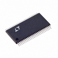
LTC1744IFW#TR Linear Technology, LTC1744IFW#TR Datasheet - Page 19

LTC1744IFW#TR
Manufacturer Part Number
LTC1744IFW#TR
Description
IC ADC 14BIT 50MSPS 48-TSSOP
Manufacturer
Linear Technology
Datasheet
1.LTC1744CFWPBF.pdf
(24 pages)
Specifications of LTC1744IFW#TR
Number Of Bits
14
Sampling Rate (per Second)
50M
Data Interface
Parallel
Number Of Converters
1
Power Dissipation (max)
1.5W
Voltage Supply Source
Single Supply
Operating Temperature
-40°C ~ 85°C
Mounting Type
Surface Mount
Package / Case
48-TFSOP (0.240", 6.10mm Width)
Lead Free Status / RoHS Status
Contains lead / RoHS non-compliant
Other names
LTC1744IFWTR
Available stocks
Company
Part Number
Manufacturer
Quantity
Price
APPLICATIO S I FOR ATIO
Output Driver Power
Separate output power and ground pins allow the output
drivers to be isolated from the analog circuitry. The power
supply for the digital output buffers, OV
to the same power supply as for the logic being driven. For
example if the converter is driving a DSP powered by a 3V
supply then OV
OV
outputs will swing between OGND and OV
Output Enable
The outputs may be disabled with the output enable pin,
OE. OE low disables all data outputs including OF and
CLKOUT. The data access and bus relinquish times are too
slow to allow the outputs to be enabled and disabled
during full speed operation. The output Hi-Z state is
intended for use during long periods of inactivity.
GROUNDING AND BYPASSING
The LTC1744 requires a printed circuit board with a clean
unbroken ground plane. A multilayer board with an inter-
nal ground plane is recommended. The pinout of the
LTC1744 has been optimized for a flowthrough layout so
that the interaction between inputs and digital outputs is
minimized. Layout for the printed circuit board should
ensure that digital and analog signal lines are separated as
much as possible. In particular, care should be taken not
to run any digital track alongside an analog signal track, an
encode signal track or underneath the ADC.
High quality ceramic bypass capacitors should be used at
the V
shown in the block diagram on the front page of this data
sheet. Bypass capacitors must be located as close to the
pins as possible. Of particular importance are the capaci-
tors between REFHA and REFLB and between REFHB and
REFLA. These capacitors should be as close to the device
as possible (1.5mm or less). Size 0402 ceramic capacitors
DD
DD,
can be powered with any voltage up to 5V. The logic
V
CM
, REFHA, REFHB, REFLA and REFLB pins as
DD
should be tied to that same 3V supply.
U
U
W
DD
, should be tied
DD
.
U
are recomended. The large 4.7 F capacitor between REFHA
and REFLA can be somewhat further away. The traces
connecting the pins and bypass capacitors must be kept
short and should be made as wide as possible.
The LTC1744 differential inputs should run parallel and
close to each other. The input traces should be as short as
possible to minimize capacitance and to minimize noise
pickup.
An analog ground plane separate from the digital process-
ing system ground should be used. All ADC ground pins
labeled GND should connect to this plane. All ADC V
bypass capacitors, reference bypass capacitors and input
filter capacitors should connect to this analog plane. The
LTC1744 has three output driver ground pins, labeled
OGND (Pins 27, 38 and 47). These grounds should con-
nect to the digital processing system ground. The output
driver supply, OV
processing system supply. OV
bypass to the digital system ground. The digital process-
ing system ground should connected to the analog plane
at ADC OGND (Pin 38).
HEAT TRANSFER
Most of the heat generated by the LTC1744 is transferred
from the die through the package leads onto the printed
circuit board. In particular, ground pins 12, 13, 36 and 37
are fused to the die attach pad. These pins have the lowest
thermal resistance between the die and the outside envi-
ronment. It is critical that all ground pins are connected to
a ground plane of sufficient area. The layout of the evalu-
ation circuit shown on the following pages has a low ther-
mal resistance path to the internal ground plane by using
multiple vias near the ground pins. A ground plane of this
size results in a thermal resistance from the die to ambient
of 35 C/W. Smaller area ground planes or poorly connected
ground pins will result in higher thermal resistance.
DD
should be connected to the digital
DD
bypass capacitors should
LTC1744
19
1744f
DD


