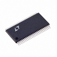
LTC1744IFW#TR Linear Technology, LTC1744IFW#TR Datasheet - Page 4

LTC1744IFW#TR
Manufacturer Part Number
LTC1744IFW#TR
Description
IC ADC 14BIT 50MSPS 48-TSSOP
Manufacturer
Linear Technology
Datasheet
1.LTC1744CFWPBF.pdf
(24 pages)
Specifications of LTC1744IFW#TR
Number Of Bits
14
Sampling Rate (per Second)
50M
Data Interface
Parallel
Number Of Converters
1
Power Dissipation (max)
1.5W
Voltage Supply Source
Single Supply
Operating Temperature
-40°C ~ 85°C
Mounting Type
Surface Mount
Package / Case
48-TFSOP (0.240", 6.10mm Width)
Lead Free Status / RoHS Status
Contains lead / RoHS non-compliant
Other names
LTC1744IFWTR
Available stocks
Company
Part Number
Manufacturer
Quantity
Price
DIGITAL I PUTS A D DIGITAL OUTPUTS
POWER REQUIRE E TS
TI I G CHARACTERISTICS
LTC1744
operating temperature range, otherwise specifications are at T
SYMBOL
V
V
I
C
V
V
I
C
I
I
range, otherwise specifications are at T
SYMBOL
V
I
P
OV
range, otherwise specifications are at T
SYMBOL
f
t
t
t
t
t
t
t
t
Note 1: Absolute Maximum Ratings are those values beyond which the life
of a device may be impaired.
Note 2: All voltage values are with respect to ground with GND
(unless otherwise noted).
Note 3: When these pin voltages are taken below GND or above V
will be clamped by internal diodes. This product can handle input currents
of greater than 100mA below GND or above V
Note 4: When these pin voltages are taken below GND, they will be
clamped by internal diodes. This product can handle input currents of
>100mA below GND without latchup. These pins are not clamped to V
4
IN
OZ
SOURCE
SINK
DD
SAMPLE(MAX)
1
2
3
4
5
6
7
8
IH
IL
IN
OH
OL
OZ
DD
DIS
DD
W
U
PARAMETER
High Level Input Voltage
Low Level Input Voltage
Digital Input Current
Digital Input Capacitance
High Level Output Voltage
Low Level Output Voltage
Hi-Z Output Leakage D13 to D0
Hi-Z Output Capacitance D13 to D0
Output Source Current
Output Sink Current
PARAMETER
Maximum Sampling Frequency
ENC Low Time
ENC High Time
Aperture Delay of Sample-and-Hold
ENC to Data Delay
ENC to CLKOUT Delay
CLKOUT to Data Delay
DATA Access Time After OE
BUS Relinquish Time
Data Latency
PARAMETER
Positive Supply Voltage
Positive Supply Current
Power Dissipation
Digital Output Supply Voltage
U
W U
U
A
A
DD
= 25 C. (Note 5)
= 25 C. (Note 5)
without latchup.
CONDITIONS
V
V
V
MSBINV and OE Only
OV
OV
V
V
V
OE = High (Note 8)
CONDITIONS
The
DD
DD
IN
OUT
OUT
OUT
CONDITIONS
(Note 9)
(Note 9)
C
C
C
C
(Note 8)
DD
DD
L
L
L
L
= 0V to V
= 5.25V
= 4.75V
= 10pF (Note 8)
= 10pF (Note 8)
= 10pF (Note 8)
= 10pF (Note 8)
The
= 0V to V
= 0V
= 5V
= 4.75V
= 4.75V
indicates specifications which apply over the full operating temperature
DD
, they
indicates specifications which apply over the full operating temperature
DD
DD
DD
A
.
, OE = High
= 25 C. (Note 5)
Note 5: V
sine wave, input range = 1.6V differential, unless otherwise specified.
Note 6: Integral nonlinearity is defined as the deviation of a code from a
straight line passing through the actual endpoints of the transfer curve.
The deviation is measured from the center of the quantization band.
Note 7: Bipolar offset is the offset voltage measured from – 0.5 LSB
when the output code flickers between 00 0000 0000 0000 and 11
1111 1111 1111.
Note 8: Guaranteed by design, not subject to test.
Note 9: Recommended operating conditions.
The
DD
I
I
I
I
O
O
O
O
= 5V, f
= –10 A
= – 200 A
= 160 A
= 1.6mA
indicates specifications which apply over the full
SAMPLE
= 50MHz, differential ENC/ENC = 2V
MIN
4.75
MIN
MIN
2.4
9.5
9.5
1.4
0.5
0.5
50
4
0
4.74
0.05
TYP
– 50
TYP
TYP
245
1.5
0.1
1.2
4.5
2.3
2.2
50
10
10
10
10
0
5
1000
1000
MAX
MAX
MAX
5.25
300
V
0.8
0.4
1.5
15
25
25
10
10
8
5
DD
P-P
50MHz
UNITS
UNITS
UNITS
cycles
MHz
1744f
mA
mA
mA
pF
pF
ns
ns
ns
ns
ns
ns
ns
ns
W
V
V
A
V
V
V
V
A
V
V


