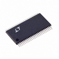
LTC1744IFW#TR Linear Technology, LTC1744IFW#TR Datasheet - Page 9

LTC1744IFW#TR
Manufacturer Part Number
LTC1744IFW#TR
Description
IC ADC 14BIT 50MSPS 48-TSSOP
Manufacturer
Linear Technology
Datasheet
1.LTC1744CFWPBF.pdf
(24 pages)
Specifications of LTC1744IFW#TR
Number Of Bits
14
Sampling Rate (per Second)
50M
Data Interface
Parallel
Number Of Converters
1
Power Dissipation (max)
1.5W
Voltage Supply Source
Single Supply
Operating Temperature
-40°C ~ 85°C
Mounting Type
Surface Mount
Package / Case
48-TFSOP (0.240", 6.10mm Width)
Lead Free Status / RoHS Status
Contains lead / RoHS non-compliant
Other names
LTC1744IFWTR
Available stocks
Company
Part Number
Manufacturer
Quantity
Price
PI FU CTIO S
SENSE (Pin 1): Reference Sense Pin. Ground selects
1.6V applied to the SENSE pin selects an input range of
V
Bypass to ground with 4.7 F ceramic chip capacitor.
GND (Pins 3, 6, 9, 12, 13, 16, 19, 21, 36, 37): ADC
Power Ground.
A
A
V
with 1 F ceramic chip capacitor.
REFLB (Pin 10): ADC Low Reference. Bypass to Pin 11 with
0.1 F ceramic chip capacitor. Do not connect to Pin 14.
REFHA (Pin 11): ADC High Reference. Bypass to Pin 10 with
0.1 F ceramic chip capacitor, to Pin 14 with a 4.7 F ceramic
capacitor and to ground with 1 F ceramic capacitor.
REFLA (Pin 14): ADC Low Reference. Bypass to Pin 15 with
0.1 F ceramic chip capacitor, to Pin 11 with a 4.7 F ceramic
capacitor and to ground with 1 F ceramic capacitor.
REFHB (Pin 15): ADC High Reference. Bypass to Pin 14 with
0.1 F ceramic chip capacitor. Do not connect to Pin 11.
TYPICAL PERFOR A CE CHARACTERISTICS
1V. V
V
CM
IN
IN
DD
SENSE
U
+
–
(Pins 7, 8, 17, 18, 20): 5V Supply. Bypass to AGND
(Pin 2): 2.5V Output and Input Common Mode Bias.
(Pin 4): Positive Differential Analog Input.
(Pin 5): Negative Differential Analog Input.
DD
, 1.6V is the largest valid input range.
selects 1.6V. Greater than 1V and less than
U
–100
–110
–120
–130
–140
–150
–10
–20
–30
–40
–50
–60
–70
–80
–90
0.5
0
Input = 5MHz, –25dBFS, No Dither
U
T
A
2 4 6
= 25 C
W
FREQUENCY (MHz)
8
10 12 14
U
16
18 20 22 24
1744 G36
24.99
MSBINV (Pin 22): MSB Inversion Control. Low inverts
the MSB, 2’s complement output format. High does not
invert the MSB, offset binary output format.
ENC (Pin 23): Encode Input. The input sample starts on
the positive edge.
ENC (Pin 24): Encode Complement Input. Conversion
starts on the negative edge. Bypass to ground with 0.1 F
ceramic for single-ended encode signal.
OE (Pin 25): Output Enable. Low enables outputs. Logic
high makes outputs Hi-Z.
CLKOUT (Pin 26): Data Valid Output. Latch data on the
rising edge of CLKOUT.
OGND (Pins 27, 38, 47): Output Driver Ground.
D0-D3 (Pins 28 to 31): Digital Outputs. D0 is the LSB.
OV
ers. Bypass to ground with 0.1 F ceramic chip capacitor.
D4-D6 (Pins 33 to 35): Digital Outputs.
D7-D10 (Pins 39 to 42): Digital Outputs.
D11-D13 (Pins 44 to 46): Digital Outputs. D13 is the MSB.
OF (Pin 48): Over/Under Flow Output. High when an over
or under flow has occurred.
DD
–100
–110
–120
–130
–140
–150
(Pins 32, 43): Positive Supply for the Output Driv-
–10
–20
–30
–40
–50
–60
–70
–80
–90
0.5
0
Input = 5MHz, –25dBFS,
Dither Applied
T
A
2 4 6
= 25 C
(Note 5)
FREQUENCY (MHz)
8
10 12 14
16
18 20 22 24
1744 G37
24.99
LTC1744
9
1744f


