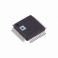
AD7484BSTZ Analog Devices Inc, AD7484BSTZ Datasheet - Page 12

AD7484BSTZ
Manufacturer Part Number
AD7484BSTZ
Description
IC ADC 14BIT SAR 3MSPS 48-LQFP
Manufacturer
Analog Devices Inc
Datasheet
1.AD7484BSTZ.pdf
(20 pages)
Specifications of AD7484BSTZ
Data Interface
Parallel
Number Of Bits
14
Sampling Rate (per Second)
3M
Number Of Converters
1
Power Dissipation (max)
90mW
Voltage Supply Source
Analog and Digital
Operating Temperature
-40°C ~ 85°C
Mounting Type
Surface Mount
Package / Case
48-LQFP
Resolution (bits)
14bit
Sampling Rate
3MSPS
Input Channel Type
Single Ended
Supply Voltage Range - Analog
4.75V To 5.25V
Supply Voltage Range - Digital
4.75V To 5.25V
Lead Free Status / RoHS Status
Lead free / RoHS Compliant
For Use With
EVAL-AD7484CBZ - BOARD EVALUATION FOR AD7484
Lead Free Status / RoHS Status
Lead free / RoHS Compliant, Lead free / RoHS Compliant
Available stocks
Company
Part Number
Manufacturer
Quantity
Price
Company:
Part Number:
AD7484BSTZ
Manufacturer:
ADI30
Quantity:
221
Company:
Part Number:
AD7484BSTZ
Manufacturer:
Analog Devices Inc
Quantity:
10 000
Part Number:
AD7484BSTZ
Manufacturer:
ADI/亚德诺
Quantity:
20 000
AD7484
Figure 11 shows the analog input circuit used to obtain the data
for the FFT plot shown in Figure 3. The circuit uses the Analog
Devices AD829 op amp as the input buffer. A bipolar analog
signal is applied as shown and biased up with a stable, low noise
dc voltage connected to the labeled terminal shown. A 220 pF
compensation capacitor is connected between Pin 5 of the
AD829 and the analog ground plane. The AD829 is supplied
with +12 V and −12 V supplies. The supply pins are decoupled
as close to the device as possible, with both a 0.1 µF and 10 µF
capacitor connected to each pin. In each case, the 0.1 µF
capacitor should be the closer of the two caps to the device.
More information on the AD829 is available at:
www.analog.com.
For higher input bandwidth applications, the Analog Devices
AD8021 op amp (also available as a dual AD8022 op amp) is the
recommended choice to drive the AD7484. Figure 12 shows the
analog input circuit used to obtain the data for the FFT plot
shown in Figure 4. A bipolar analog signal is applied to the
terminal shown and biased up with a stable, low noise dc
voltage connected as shown. A 10 pF compensation capacitor is
connected between Pin 5 of the AD8021 and the negative
supply. As with the previous circuit, the AD8021 is supplied
with +12 V and −12 V supplies. The supply pins are decoupled
as close to the device as possible, with both a 0.1 µF and 10 µF
capacitor connected to each pin. In each case, the 0.1 µF
capacitor should be the closer of the two caps to the device. The
AD8021 logic reference pin is tied to analog ground, and the
DISABLE pin is tied to the positive supply as shown. Detailed
information on the AD8021 is available at: www.analog.com.
VOLTAGE
SIGNAL
BIAS
AC
Figure 11. Analog Input Circuit Used for 10 kHz Input Tone
Figure 12. Analog Input Circuit Used for 1 MHz Input Tone
VOLTAGE
SIGNAL
1k Ω
1k Ω
BIAS
AC
100 Ω
220 Ω
50 Ω
3
2
150 Ω
+
–
AD829
1
2
3
8
+
–
1
AD8021
+V
5
8
220 Ω
7
10pF
S
220pF
–V
5
+V
10pF
4
S
7
S
–V
6
4
S
6
V
IN
V
IN
Rev. A | Page 12 of 20
CIRCUIT DESCRIPTION
Converter Operation
The AD7484 is a 14-bit algorithmic successive approximation
analog-to-digital converter based around a capacitive DAC. It
provides the user with track-and-hold, reference, an ADC, and
versatile interface logic functions on a single chip. The normal
analog input signal range that the AD7484 can convert is 0 V to
2.5 V. By using the offset and overrange features on the ADC,
the AD7484 can convert analog input signals from −200 mV to
+2.7 V while operating from a single 5 V supply. The part
requires a 2.5 V reference, which can be provided from the
part’s own internal reference or an external reference source.
Figure 13 shows a simplified schematic of the ADC. The control
logic, SAR, and capacitive DAC are used to add and subtract
fixed amounts of charge from the sampling capacitor to bring
the comparator back to a balanced condition.
Conversion is initiated on the AD7484 by pulsing the CONVST
input. On the falling edge of CONVST , the track-and-hold goes
from track mode to hold mode and the conversion sequence is
started. Conversion time for the part is 300 ns. Figure 14 shows
the ADC during conversion. When conversion starts, SW2 will
open and SW1 will move to Position B, causing the comparator
to become unbalanced. The ADC then runs through its
successive approximation routine and brings the comparator
back into a balanced condition. When the comparator is
rebalanced, the conversion result is available in the SAR
Register.
AGND
V
IN
SW1
A
CONTROL
Figure 13. Simplified Block Diagram of AD7484
B
INPUTS
V
REF
V
IN
Figure 14. ADC Conversion Phase
CAPACITIVE
SWITCHES
CONTROL
SW2
LOGIC
SAR
DAC
COMPARATOR
14-BIT PARALLEL
+
–
OUTPUT DATA
COMPARATOR
CONTROL LOGIC
CAPACITIVE
DAC


