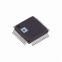
AD7484BSTZ Analog Devices Inc, AD7484BSTZ Datasheet - Page 8

AD7484BSTZ
Manufacturer Part Number
AD7484BSTZ
Description
IC ADC 14BIT SAR 3MSPS 48-LQFP
Manufacturer
Analog Devices Inc
Datasheet
1.AD7484BSTZ.pdf
(20 pages)
Specifications of AD7484BSTZ
Data Interface
Parallel
Number Of Bits
14
Sampling Rate (per Second)
3M
Number Of Converters
1
Power Dissipation (max)
90mW
Voltage Supply Source
Analog and Digital
Operating Temperature
-40°C ~ 85°C
Mounting Type
Surface Mount
Package / Case
48-LQFP
Resolution (bits)
14bit
Sampling Rate
3MSPS
Input Channel Type
Single Ended
Supply Voltage Range - Analog
4.75V To 5.25V
Supply Voltage Range - Digital
4.75V To 5.25V
Lead Free Status / RoHS Status
Lead free / RoHS Compliant
For Use With
EVAL-AD7484CBZ - BOARD EVALUATION FOR AD7484
Lead Free Status / RoHS Status
Lead free / RoHS Compliant, Lead free / RoHS Compliant
Available stocks
Company
Part Number
Manufacturer
Quantity
Price
Company:
Part Number:
AD7484BSTZ
Manufacturer:
ADI30
Quantity:
221
Company:
Part Number:
AD7484BSTZ
Manufacturer:
Analog Devices Inc
Quantity:
10 000
Part Number:
AD7484BSTZ
Manufacturer:
ADI/亚德诺
Quantity:
20 000
AD7484
Table 4. Pin Function Descriptions
Pin No.
1, 5, 13, 46
2
3, 4, 6, 11, 12,
14, 15, 47, 48
7
8
9
10
16
17
18
19
20
21
22 to 28,
33 to 39
29
30, 31
32
40
41
42
43
44
45
Mnemonic
AV
C
AGND
VIN
REFOUT
REFIN
REFSEL
STBY
NAP
CS
RD
WRITE
BUSY
D0 to D13
DV
DGND
V
D14
CONVST
RESET
MODE2
MODE1
CLIP
BIAS
DRIVE
DD
DD
Description
Positive Power Supply for Analog Circuitry.
Decoupling Pin for Internal Bias Voltage. A 1 nF capacitor should be placed between this pin and AGND.
Power Supply Ground for Analog Circuitry.
Analog Input. Single-ended analog input channel.
Reference Output. REFOUT connects to the output of the internal 2.5 V reference buffer.
A 470 nF capacitor must be placed between this pin and AGND.
Reference Input. A 470 nF capacitor must be placed between this pin and AGND.
When using an external voltage reference source, the reference voltage should be applied to this pin.
Reference Decoupling Pin. When using the internal reference, a 1 nF capacitor must be connected from
this pin to AGND. When using an external reference source, this pin should be connected directly to AGND.
Standby Logic Input. When this pin is logic high, the device will be placed in standby mode.
See the Power Saving section for further details.
NAP Logic Input. When this pin is logic high, the device will be placed in a very low power mode.
See the Power Saving section for further details.
Chip Select Logic Input. This pin is used in conjunction with RD to access the conversion result. The
data bus is brought out of three-state and the current contents of the output register driven onto the
data lines following the falling edge of both CS and RD . CS is also used in conjunction with WRITE to
perform a write to the offset register. CS can be hardwired permanently low.
Read Logic Input. Used in conjunction with CS to access the conversion result.
Write Logic Input. Used in conjunction with CS to write data to the offset register. When the desired offset
word has been placed on the data bus, the WRITE line should be pulsed high. It is the falling edge of this
pulse that latches the word into the offset register.
Busy Logic Output. This pin indicates the status of the conversion process. The BUSY signal goes low
after the falling edge of CONVST and stays low for the duration of the conversion. In Parallel Mode 1,
the BUSY signal returns high when the conversion result has been latched into the output register.
In Parallel Mode 2, the BUSY signal returns high as soon as the conversion has been completed, but the
conversion result does not get latched into the output register until the falling edge of the next CONVST
pulse.
Data I/O Bits (D13 is MSB). These are three-state pins that are controlled by CS , RD , and WRITE.
The operating voltage level for these pins is determined by the V
Positive Power Supply for Digital Circuitry.
Ground Reference for Digital Circuitry.
Logic Power Supply Input. The voltage supplied at this pin will determine at what voltage the
interface logic of the device will operate.
Data Output Bit for Overranging. If the overrange feature is not used, this pin should be pulled
to DGND via a 100 kΩ resistor.
Convert Start Logic Input. A conversion is initiated on the falling edge of the CONVST signal. The input
track-and-hold amplifier goes from track mode to hold mode and the conversion process commences.
Reset Logic Input. An active low reset pulse must be applied to this pin after power-up to ensure correct
operation. A falling edge on this pin resets the internal state machine and terminates a conversion that
may be in progress. The contents of the offset register will also be cleared on this edge. Holding this pin low
keeps the part in a reset state.
Operating Mode Logic Input. See Table 7 for details.
Operating Mode Logic Input. See Table 7 for details.
Logic Input. A logic high on this pin enables output clipping. In this mode, any input voltage that
is greater than positive full scale or less than negative full scale will be clipped to all 1s or all 0s,
respectively. Further details are given in the Offset/Overrange section.
Rev. A | Page 8 of 20
DRIVE
input.


