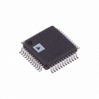
AD7484BSTZ Analog Devices Inc, AD7484BSTZ Datasheet - Page 15

AD7484BSTZ
Manufacturer Part Number
AD7484BSTZ
Description
IC ADC 14BIT SAR 3MSPS 48-LQFP
Manufacturer
Analog Devices Inc
Datasheet
1.AD7484BSTZ.pdf
(20 pages)
Specifications of AD7484BSTZ
Data Interface
Parallel
Number Of Bits
14
Sampling Rate (per Second)
3M
Number Of Converters
1
Power Dissipation (max)
90mW
Voltage Supply Source
Analog and Digital
Operating Temperature
-40°C ~ 85°C
Mounting Type
Surface Mount
Package / Case
48-LQFP
Resolution (bits)
14bit
Sampling Rate
3MSPS
Input Channel Type
Single Ended
Supply Voltage Range - Analog
4.75V To 5.25V
Supply Voltage Range - Digital
4.75V To 5.25V
Lead Free Status / RoHS Status
Lead free / RoHS Compliant
For Use With
EVAL-AD7484CBZ - BOARD EVALUATION FOR AD7484
Lead Free Status / RoHS Status
Lead free / RoHS Compliant, Lead free / RoHS Compliant
Available stocks
Company
Part Number
Manufacturer
Quantity
Price
Company:
Part Number:
AD7484BSTZ
Manufacturer:
ADI30
Quantity:
221
Company:
Part Number:
AD7484BSTZ
Manufacturer:
Analog Devices Inc
Quantity:
10 000
Part Number:
AD7484BSTZ
Manufacturer:
ADI/亚德诺
Quantity:
20 000
The effect of writing a negative value to the offset register is
shown in Figure 22 If a value of −512 was written to the offset
register, the bottom end reference point now occurs at
Following this, the analog input voltage needed to produce a
full-scale (0x3FFF) result from the ADC is now
Table 5 shows the expected ADC result for a given analog input
voltage with different offset values and with CLIP tied to logic
high. The combined advantages of the offset and overrange
features of the AD7484 are shown clearly in Table 6. It shows
the same range of analog input and offset values, as shown in
Table 5 but with the clipping feature disabled.
Table 5. Clipping Enabled (CLIP = 1)
Offset VIN
−200 mV
−156.3 mV
0 V
+78.2 mV
+2.3435 V
+2.5 V
+2.5779 V
+2.7 V
Table 6. Clipping Disabled (CLIP = 0)
Offset VIN
−200 mV
−156.3 mV
0 V
+78.2 mV
+2.3435 V
+2.5 V
+2.5779 V
+2.7 V
0
2
.
.
5
5
V
LSB
Figure 22. Transfer Characteristic with Negative Offset
−
1
111...111
111...110
111...000
011...111
000...010
000...001
000...000
.
−
5
(
LSB
−
512
−512
0
0
0
0
14846
15871
16383
16383
−512
−1823
−1536
−512
0
14846
15872
16383
17183
−
0V
(
LSB
−
512
1LSB = V
–OFFSET
0.5LSB
)
ADC DATA, D[0:13]
ADC DATA, D[0:13]
=
LSB
78
ANALOG INPUT
REF
.
0
0
0
0
512
15358
16383
16383
16383
)
0
−1311
−1024
0
512
15358
16384
16895
17695
20
=
/16384
2
mW
.
5779
V
+V
REF
–OFFSET
+1024
0
0
1024
1536
16383
16383
16383
16383
+1024
−287
0
1024
1536
16382
17408
17919
18719
– 1.5LSB
D14
1 1 1
1 1 0
1 0 0
0 0 0
0 0 0
0 0 1
0 1 1
1 1 1
Rev. A | Page 15 of 20
Values from −1310 to +1310 may be written to the offset
register. These values correspond to an offset of ±200 mV. A
write to the offset register is performed by writing a 13-bit
word to the part, as detailed in the Parallel Interface section.
The 12 LSBs of the 15-bit word contain the offset value, while
the 3 MSBs must be set to 0. Failure to write 0s to the 3 MSBs
may result in incorrect operation of the device.
PARALLEL INTERFACE
The AD7484 features two parallel interfacing modes. These
modes are selected by the mode pins (see Table 7).
Table 7. Table III. Operating Modes
Do Not Use
Parallel Mode 1
Parallel Mode 2
Do Not Use
In Parallel Mode 1, the data in the output register is updated on
the rising edge of BUSY at the end of a conversion and is
available for reading almost immediately afterwards. Using this
mode, throughput rates of up to 2.5 MSPS can be achieved. This
mode should be used if the conversion data is required
immediately after the conversion has completed. An example
where this may be of use is if the AD7484 is operating at much
lower throughput rates with the NAP mode (for power-saving
reasons), and the input signal is being compared with set limits
within the DSP or other controller. If the limits are exceeded,
the ADC is brought immediately into full power operation and
commences sampling at full speed. Figure 31 shows a timing
diagram for the AD7484 operating in Parallel Mode 1 with both
CS and RD tied low.
In Parallel Mode 2, the data in the output register is not updated
until the next falling edge of CONVST . This mode could be
used where a single sample delay is not vital to the system
operation and conversion speeds of greater than 2.5 MSPS are
desired. This may occur, for example, in a system where a large
amount of samples are taken at high speed before a Fast Fourier
Transform is performed for frequency analysis of the input
signal. Figure 32 shows a timing diagram for the AD7484
operating in Parallel Mode 2 with both CS and RD tied low.
Data must not be read from the AD7484 while a conversion is
taking place. For this reason, if operating the AD7484 at
throughput speeds greater than 2.5 MSPS, it will be necessary to
tie both the CS and RD pins on the AD7484 low and use a
buffer on the data lines. This situation may also arise in the case
where a read operation cannot be completed in the time after
the end of one conversion and the start of the quiet period
before the next conversion.
MODE2
0
0
1
1
MODE1
0
1
0
1
AD7484


